Connection terminal and a semiconductor device including at least one connection terminal

a technology of connection terminals and semiconductor devices, which is applied in the direction of coupling device details, coupling device connections, coupling contact members, etc., can solve the problems of large number of terminals and fine pitch, disadvantageous ball bump processes, and high production costs, and achieves small width, low investment and manufacturing costs, and sufficient adhesion strength

Inactive Publication Date: 2005-06-21
TAIWAN SEMICON MFG CO LTD
View PDF21 Cites 23 Cited by
  • Summary
  • Abstract
  • Description
  • Claims
  • Application Information

AI Technical Summary

Benefits of technology

[0016]The present invention has objectives to offer connection terminals structured so suitably to the manufacture by electroless plating which requires less investment and manufacturing cost than electrop

Problems solved by technology

However, problems arise where manufacturing equipment, such as a sputtering device and a photo device, is needed apart from an electroplating device, because the processes require formation of a barrier metal layer which doubles as a conductive film in electroplating and of windows for bump formation by the coating, exposure, and development of a photoresist.
This indicates that ball bump processes are disadvantageous in achieving large numbers of terminals and a fine pitch.
Problems do exist however in a conventional arrangement of connection terminals where bumps are formed by

Method used


Image

  • Connection terminal and a semiconductor device including at least one connection terminal
  • Connection terminal and a semiconductor device including at least one connection terminal
  • Connection terminal and a semiconductor device including at least one connection terminal

Examples


example 1

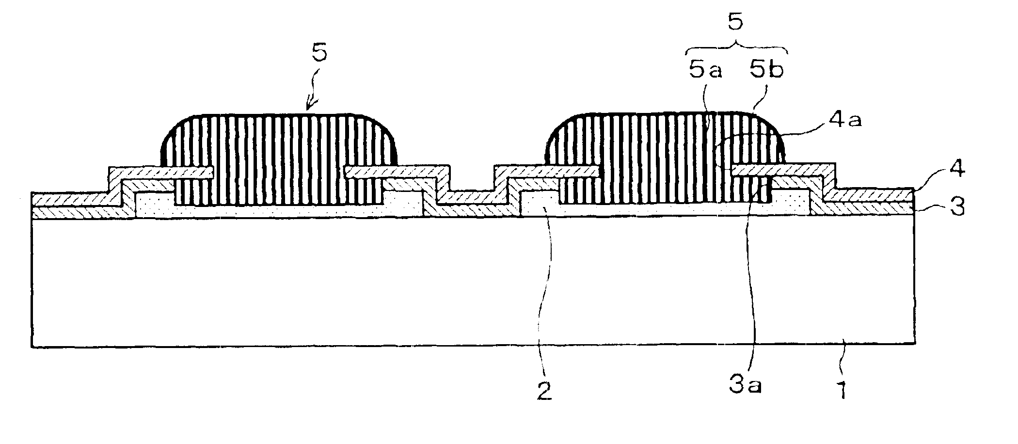
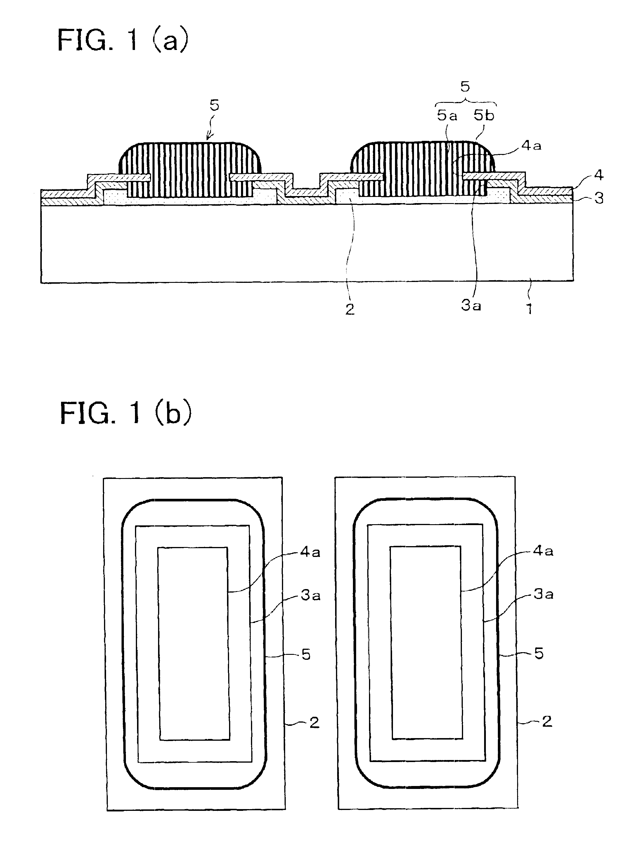
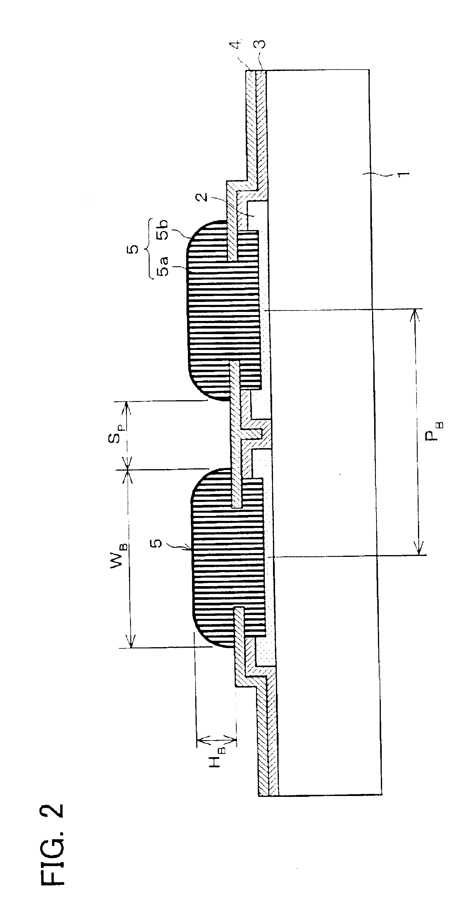
[0066]FIG. 2 shows an arrangement of connection terminal parts of a semiconductor device as example 1. The arrangement is basically the same as the structure of the connection terminal parts described in the embodiment in reference to FIG. 1. That is, there are provided an insulating film and active elements (neither shown), electrode pads 2, a first protection film 3, and a second protection film 4 formed in this order on a semiconductor substrate 1. A bump 5 is formed in an opening 3a in the first protection film 3 on an electrode pad 2 and an opening 4a in the second protection film 4 on the first protection film 3. Each bump 5 is made up of a bump main body 5a and a surface film 5b.

[0067]In the present example, each opening 3a in the first protection film 3 measures 25 μm by 70 μm, and each opening 4a in the second protection film 4 measures 15 μm by 60 μm. The bump main bodies 5a are formed as a 10 μm high NiP layer (7-11% phosphorus), and the surface films 5b are formed as a ...


PUM


Abstract

A first protection film (3) and a second protection film (4) are formed on an electrode pad (2). Bumps (5) are formed at sites where the deposited first and second protection films (3), (4) are both removed. The openings (3a) where the lower, first protection film (3) is removed are larger than the openings (4a) where the upper, second protection film (4) is removed, so that the upper, second protection film (4) has an overhanging structure. The bottom periphery of the bump (5) is formed to extend under the second protection film (4).

Description

FIELD OF THE INVENTION[0001]The present invention relates to connection terminals and a manufacturing method thereof, as well as a semiconductor device using the same and a manufacturing method thereof, the terminals being provided, for example, as projecting electrodes (hereinafter, “bumps”) on electrode pads to enable the semiconductor device to make electrical connections to external wires.BACKGROUND OF THE INVENTION[0002]Recent years have seen the advent of smaller and higher-performance electronics and increasing efforts to produce even smaller semiconductor devices having more terminals with a finer pitch. A result is rapidly increasing numbers of semiconductor chips (devices) packaged using a tape carrier (tape carrier package; hereinafter, “TCP”) or flip chip bonded directly onto a substrate.[0003]These types of packaging require a structure including connection bumps disposed on electrode pads of the semiconductor device, so as to provide connection terminals to the semicon...

Claims


Application Information

Patent Timeline
IPC IPC(8): H01L21/02H01L21/60H01L23/485H01L23/48
CPCH01L24/11H01L24/13H01L2224/13099H01L2924/0001H01L2224/13664H01L2224/13644H01L2224/13611H01L2224/13164H01L2224/13155H01L2224/13147H01L2224/13144H01L2224/13111H01L2924/014H01L2924/01045H01L2924/01023H01L2924/01006H01L2924/01005H01L2924/3025H01L2924/01322H01L2924/01004H01L2924/01011H01L2924/01013H01L2924/01015H01L2924/01018H01L2924/01029H01L2924/0103H01L2924/01033H01L2924/01046H01L2924/01051H01L2924/01074H01L2924/01078H01L2924/01079H01L2924/01082H01L2924/00014H01L24/05H01L2224/05557H01L2224/05567H01L2224/05573H01L2224/13018H01L2224/05599H01L21/288
Inventor ONO, ATSUSHIASAZU, TAKUROYAMAGUCHI, SHINJI
Owner TAIWAN SEMICON MFG CO LTD
Why Eureka
Try Eureka