Methods of fabricating metallic materials

Inactive Publication Date: 2005-06-21
HONEYWELL INT INC
View PDF8 Cites 71 Cited by
  • Summary
  • Abstract
  • Description
  • Claims
  • Application Information

AI Technical Summary

Benefits of technology

[0015]After the <220>-oriented texture is induced within the material of the billet, post deformation recovery annealing can be conducted to enhance the strength of the <220>-oriented textures. The post deformation recovery annealing can be conducted under conditions which maintain a sub-micron average grain size within the material of the billet. In addition to, or alternatively to, the post deformation

Problems solved by technology

Also, the extrusions can create a weak, or even tota

Method used


Image

  • Methods of fabricating metallic materials
  • Methods of fabricating metallic materials
  • Methods of fabricating metallic materials

Examples


Embodiment Construction

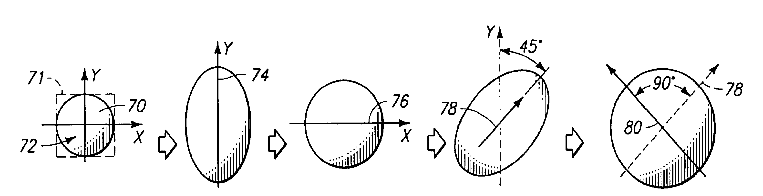
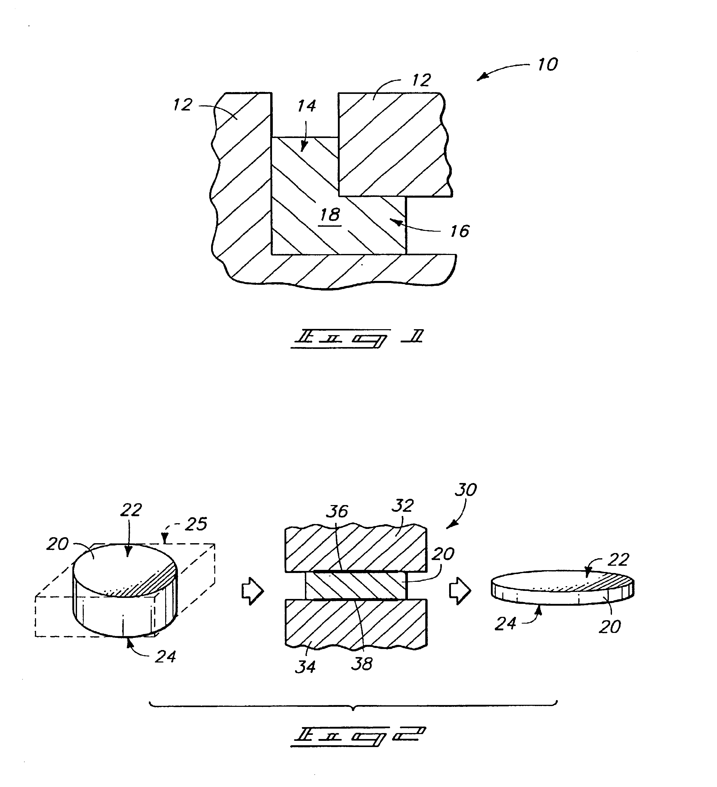
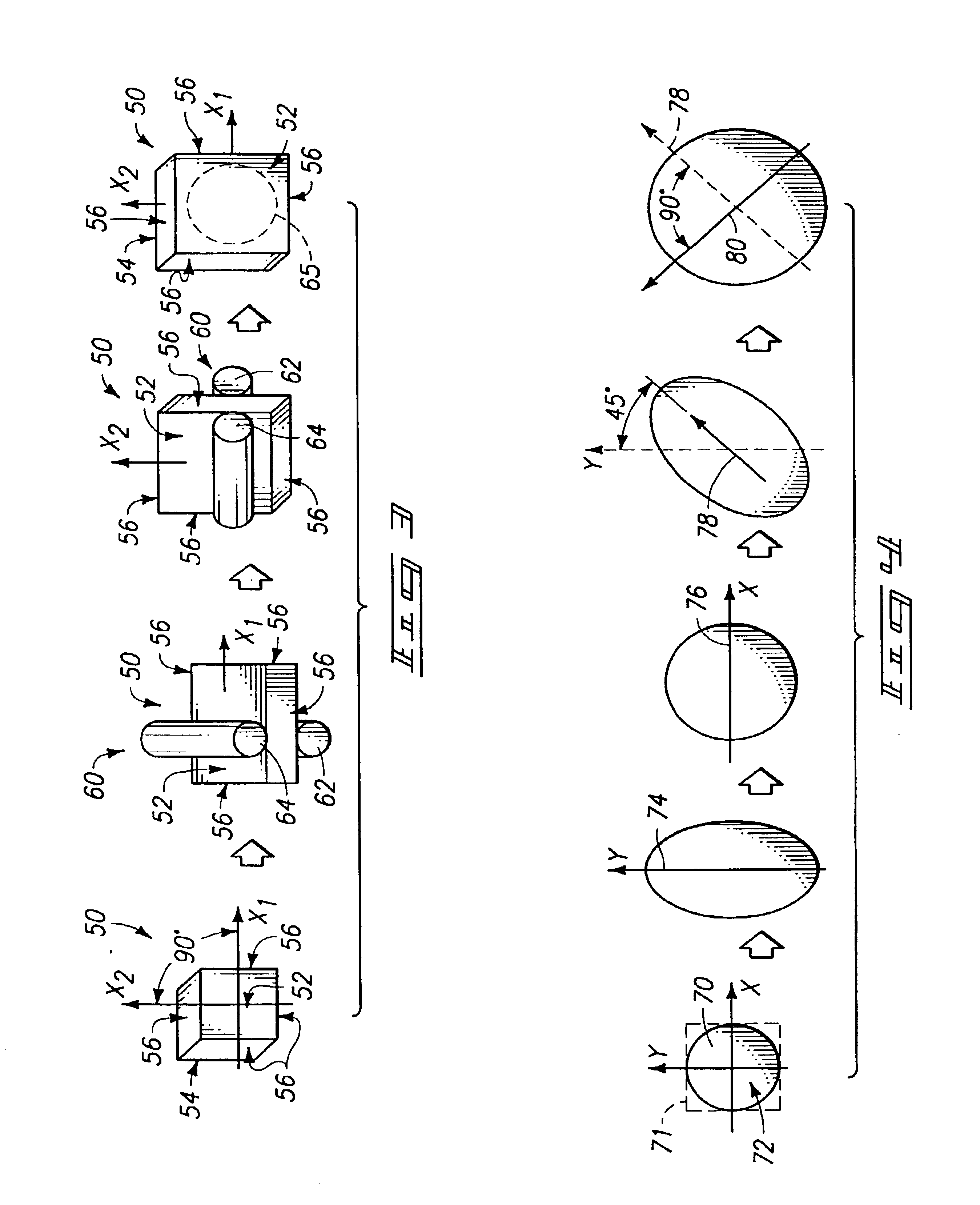
[0033]The invention encompasses a method for producing physical vapor deposition targets, such as sputtering targets, having uniform average grain sizes of less than 30 microns (preferably less than 1 micron), and axial-oriented or planar-oriented texture of controllable strength. The targets can further comprise substantially no casting defects, and in particular can comprise, for example, no (or very few) voids, particles, and inclusions. The present invention encompasses utilization of equal channel angular extrusion (ECAE) in combination with one or both of forging and cross-rolling to induce a desired texture in a metallic material. ECAE is described generally in U.S. Pat. Nos. 5,400,633; 5,513,512; 5,600,989; 5,850,755 and 5,590,389, all of which are hereby incorporated by reference in this document.

[0034]Methodology of the present invention can utilize ECAE to deform f.c.c unit cell metals and alloys. The deformation can occur at low temperature, and with a processing route ...


PUM

PropertyMeasurementUnit
Grain sizeaaaaaaaaaa
Temperatureaaaaaaaaaa

Abstract

The invention includes a physical vapor deposition target composed of a face centered cubic unit cell metal or alloy and having a uniform grain size less than 30 microns, preferably less than 1 micron; and a uniform axial or planar <220> texture. Also described is a method for making sputtering targets. The method can comprise billet preparation; equal channel angular extrusion with a prescribed route and number of passes; and cross-rolling or forging subsequent to the equal channel angular extrusion.

Description

CROSS REFERENCE TO RELATED APPLICATIONS[0001]This application is a divisional of U.S. patent application Ser. No. 09 / 705,101 which was filed on Nov. 2, 2000 and which is incorporated by reference herein.TECHNICAL FIELD[0002]The invention pertains to physical vapor deposition target compositions, and also pertains to methods for fabricating materials comprising of face-centered cubic (f.c.c.) unit cell metals or alloys.BACKGROUND OF THE INVENTION[0003]Physical vapor deposition (PVD) is a technology by which thin metallic and ceramic layers may be deposited on a substrate, and includes, for example, sputtering processes. PVD processes can be utilized in, for example, semiconductor device fabrication to form thin films of material over semiconductor substrates. A difficulty in forming thin films over semiconductor substrates can occur in attempting to maintain uniformity of film thickness and composition over an uneven topography. For instance, semiconductor substrates will frequently ...

Claims


Application Information

Patent Timeline
IPC IPC(8): C22F1/00C23C14/34C22F1/04C22C21/12C22F1/08H01J37/34H01L21/285
CPCB21C23/001C23C14/3414C22F1/00B21J1/025C23C14/00
Inventor SEGAL, VLADIMIR M.FERRASSE, STEPHANEALFORD, FRANK
Owner HONEYWELL INT INC
Why Eureka
Try Eureka