Semiconductor device and its manufacturing method

a technology of semiconductor devices and manufacturing methods, applied in semiconductor devices, semiconductor/solid-state device details, electrical apparatus, etc., can solve the problems of affecting the alignment of the contact hole, and causing the junction to be prone to excessive etching, so as to prevent the junction from etching and prevent undesirable etching

Inactive Publication Date: 2005-06-21
SONY CORP
View PDF6 Cites 6 Cited by
  • Summary
  • Abstract
  • Description
  • Claims
  • Application Information

AI Technical Summary

Benefits of technology

[0015]It is therefore an object of the invention to prevent junction leakage in an LSI device incorporating DRAM cells and logics by preventing undesirable etching of a device isolation insulating film and an impurity diffusion layer upon making a contact hole with a large aspect ratio for connecting a metal layer to

Problems solved by technology

During a long etching process, the contact hole 94 is liable to be excessively etched.
At worst, an aperture is made beyond the junction interface, inviting an increase of the junction leakage.
On the other hand, as shown in FIG. 1, in an LSI device incorporating DRAM cells and logics, it is not possible to keep a large margin for facilitating alignment between the impurity diffusion layer 93 and the contact hole 94 con

Method used


Image

  • Semiconductor device and its manufacturing method
  • Semiconductor device and its manufacturing method
  • Semiconductor device and its manufacturing method

Examples


Embodiment Construction

[0074]An embodiment of the semiconductor device according to the invention is explained below with reference to FIGS. 4 through 7B. The semiconductor device according to the invention includes DRAM memory cells and peripheral MOS transistors.

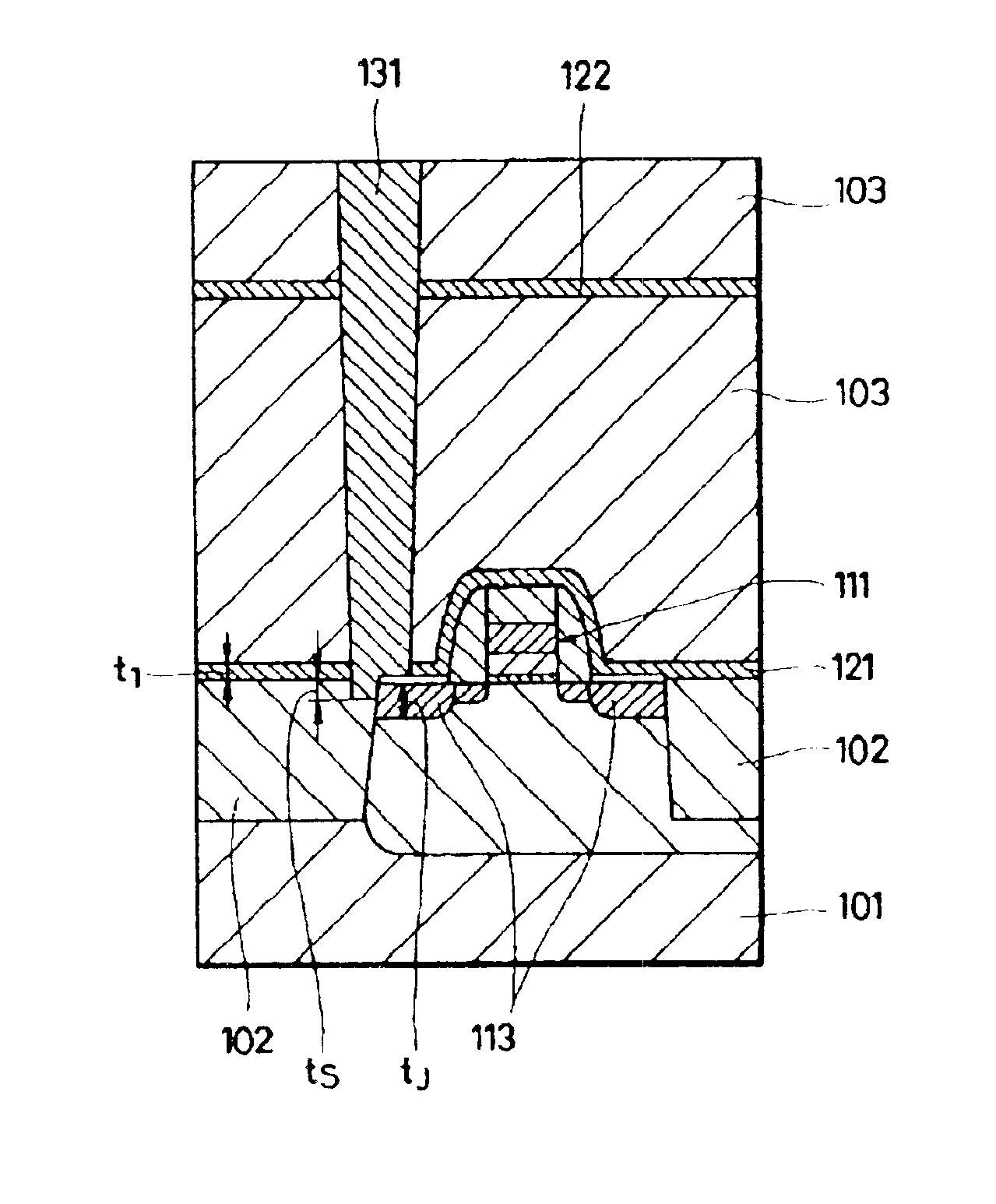
[0075]As shown in FIG. 4, a DRAM memory cell and a peripheral MOS transistor are formed in device-forming regions separated by a device isolation insulating film 102 on a semiconductor substrate 101. A first etching stopper layer 121 made of an insulating film is formed over a gate electrode 111 and impurity diffusion regions 113 of the MOS transistor region. At least one of the impurity diffusion regions 113 maybe a unitary impurity diffusion region. The first etching stopper layer 121 is made of, for example, a silicon nitride film. A second etching stopper layer 122 is formed in an upper level of a capacitor portion of the DRAM memory cell. The second etching stopper layer 122 is made of silicon nitride film, for example. Alternatively, altho...


PUM


Abstract

In a contact structure having a large aspect ratio in a LSI device incorporating DRAM cells and logics, for the purpose of preventing over-etching of a device isolation insulating film and an impurity diffusion layer and thereby minimizing junction leakage, a first etching stopper layer covering a peripheral MOS transistor and a second etching stopper layer overlying a capacitor section of a DRAM memory cell are formed. An impurity diffusion layer of the peripheral MOS transistor is connected to a metal wiring layer formed in an upper level of the capacitor section by an electrode layer extending through the first and second etching stopper layers. At least one of such impurity diffusion layers is connected to the electrode layer at its boundary with the device isolation insulating film, and depth of the bottom of the electrode layer formed on the device isolation insulating film from the surface of the impurity diffusion layer is shorter than the junction depth of the impurity diffusion layer.

Description

CROSS-REFERENCE TO RELATED APPLICATIONS[0001]This application is based upon and claims priority of U.S. patent application Ser. No. 09 / 689,392 filed on Oct. 12, 2000 now abandoned that claims priority of Japanese Patent Applications No. P11-291066, filed in Oct. 13, 1999, and Japanese Patent Application No. P2000-275912 filed in Sep. 12, 2000, the contents being incorporated herein by reference.BACKGROUND OF THE INVENTION[0002]1. Field of the Invention[0003]This invention relates to a semiconductor device and its manufacturing method and, more particularly, to a device structure and its manufacturing method for reliably making a contact connecting a metal wiring layer formed in an upper level of a capacitor of DRAM to an impurity diffusion layer and a gate electrode formed on a semiconductor substrate without increasing the junction leakage.[0004]2. Description of the Related Art[0005]A conventional LSI device incorporating DRAM cells and logics is explained below with reference to ...

Claims


Application Information

Patent Timeline
IPC IPC(8): H01L21/70H01L21/8242H01L23/485H01L23/48H01L21/768H01L27/04H01L27/108
CPCH01L23/485H01L27/10894H01L27/10855H01L27/10888H01L2924/0002H01L2924/00H10B12/0335H10B12/485H10B12/09H10B12/00
Inventor YOSHIHARA, IKUOFUTO, WATARO
Owner SONY CORP
Why Eureka
Try Eureka