
Bump forming method and apparatus for heating and compressing bump materials inserted in positioning holes

Inactive Publication Date: 2005-06-28
UMC JAPAN
View PDF8 Cites 0 Cited by
  • Summary
  • Abstract
  • Description
  • Claims
  • Application Information

AI Technical Summary

Benefits of technology

[0011]In consideration of the above circumstances, an object of the present invention is to provide a bump forming method and apparatus by which when bumps are formed at specific positions on a main surface of a semiconductor substrate, no deformed bump having an abnormal shape is formed and no shape correcting process is necessary, the member for handling the bump materials can be easily changed, and the position of the member after the change of the member can be easily adjusted with a desired accuracy, thereby shortening the bump forming process and reducing the manufacturing cost.
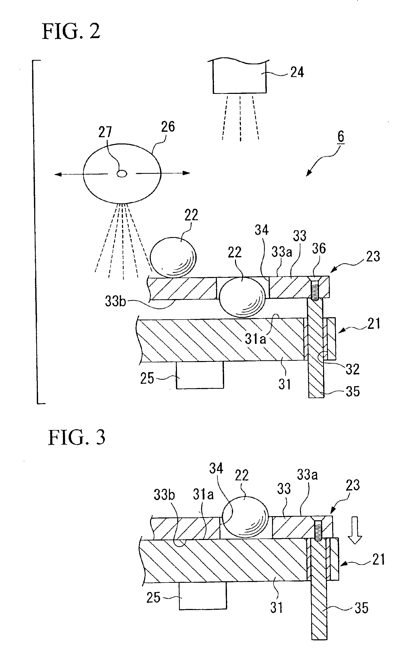
[0018]According to the above method, holding and positioning of the bump materials can be easily performed. In addition, bumps having a specific shape can be formed by a single compressing and heating operation; thus, no bump material has an abnormal shape which requires an operation for correcting the shape. Accordingly, it is possible to reduce the time for performing the bump forming process and also reduce the manufacturing cost.
[0019]The method may further comprise the step of generating ultrasonic waves toward the bump materials by using an ultrasonic oscillating device when the bump materials are heated and pressed, so as to improve contact strength between the bump materials and the semiconductor substrate.
[0024]According to the apparatus, holding and positioning of the bump materials can be easily performed. Therefore, it is possible to reduce the time for performing the bump forming process and also reduce the manufacturing cost.

Problems solved by technology

Such processing is not easy.
When the bump balls are compression-bonded all together onto a large number of bonding pads, the force for attracting the bump balls may be reduced, and as a result, it is difficult to compression-bond bump balls all together.
In addition, when bump balls are attracted to the attraction holes, the bump balls may be deformed.
Therefore, when the bonding head is changed, the position or the like of the bonding head must be adjusted again; thus, it is not easy to change the bonding head.

Method used


Image

  • Bump forming method and apparatus for heating and compressing bump materials inserted in positioning holes
  • Bump forming method and apparatus for heating and compressing bump materials inserted in positioning holes
  • Bump forming method and apparatus for heating and compressing bump materials inserted in positioning holes

Examples


Embodiment Construction

[0035]Hereinafter, embodiments of the bump forming method and apparatus according to the present invention will be explained with reference to the drawings.

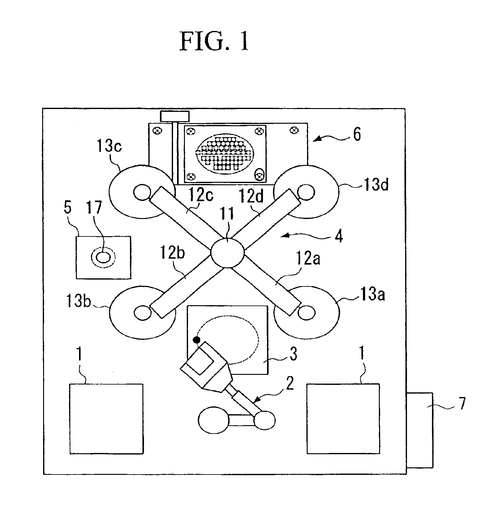
[0036]FIG. 1 is a plan view for showing a bump ball arranging and compression-bonding system for implementing the bump (ball) forming method as an embodiment of the present invention. In the figure, reference numeral 1 indicates a cassette platform, reference numeral 2 indicates a transfer robot, reference numeral 3 indicates a positioning table, reference numeral 4 indicates a cross arm, reference numeral 5 indicates an alignment unit, reference numeral 6 indicates a bonding head (i.e., a bump forming apparatus), and reference numeral 7 indicates a control panel for controlling the above elements.

[0037]The cassette platform 1 is a dedicated platform for setting a wafer cassette in which a plurality of silicon wafers (i.e., semiconductor substrates, where the silicon wafer may be simply called the wafer, hereinbelow) are containe...


PUM

PropertyMeasurementUnit
Thicknessaaaaaaaaaa
Diameteraaaaaaaaaa
Electric chargeaaaaaaaaaa

Abstract

A bump forming method and apparatus by which no deformed bump having an abnormal shape is formed and no shape correcting process is necessary, the member for handling the bump materials can be easily changed, and the position of the member after the change of the member can be easily adjusted with a desired accuracy, thereby shortening the bump forming process and reducing the manufacturing cost. A positioning member is set above a heating device. Bump materials are inserted into positioning holes of the positioning member and are made to partially protrude from the holes toward a side opposite to the heating device. A semiconductor substrate is positioned onto the positioning member so that the semiconductor substrate faces the protruding side of the bump materials. The bump materials are heated and pressed from the protruding side via the semiconductor substrate so as to form bumps having a specific shape.

Description

BACKGROUND OF THE INVENTION[0001]1. Field of the Invention[0002]The present invention relates to a bump forming method and apparatus, and in particular, relates to a method and apparatus by which when bumps are formed at specific positions on a main surface of a semiconductor substrate, no deformed bump is formed and no shape correcting process is necessary, thereby shortening the bump forming process and reducing the manufacturing cost.[0003]2. Description of the Related Art[0004]In conventional semiconductor devices such as ICs, LSIs, and VLSIs, bumps are formed at specific positions (typically, on bonding pads) on a silicon wafer (i.e., a semiconductor substrate) by compression-bonding of bump balls made of metal material, printing of metal paste, plating of metal layers, wire-bonding connection, or the like. One of these methods is selected according to the shape or size of the bumps to be formed. Here, the shape or size of the bumps necessary depends on the shape or thickness o...

Claims


Application Information

Patent Timeline
IPC IPC(8): B23P19/00H01L21/60H01L21/02H01L21/44H01L23/12B23K3/06
CPCB23K3/0623H01L24/11H01L2224/13099H01L2924/01004H01L2924/01013Y10T29/5313H01L2924/01078H01L2924/01322H01L2924/14H01L2924/01006H01L2924/01033H01L2924/01022H01L2224/05573H01L2224/05568H01L2924/00014H01L2224/05599H01L21/60
Inventor ISA, YUKIHIRO
Owner UMC JAPAN
Learn More