Antenna apparatus and communication apparatus using the same

a communication apparatus and antenna technology, applied in the field of radio communication, can solve the problems of difficult to reduce the distance between, the antenna apparatus cannot be sufficiently miniaturized, and the signal loss is difficult to be sufficiently reduced, so as to achieve the effect of sufficiently reducing the signal loss

Inactive Publication Date: 2005-06-28
UBE IND LTD
View PDF13 Cites 30 Cited by
  • Summary
  • Abstract
  • Description
  • Claims
  • Application Information

AI Technical Summary

Benefits of technology

[0007]Consequently, an object of the present invention is to provide an antenna apparatus which can further be miniaturized and in which a signal loss can sufficiently be reduced. Another object of the present invention is to provide a communication apparatus in which such an antenna apparatus is used.

Problems solved by technology

Additionally, a thickness of the dielectric substrate is further added, and therefore the antenna apparatus cannot sufficiently be miniaturized.
Since it is necessary to dispose the predetermined distance between the dielectric substrate and the radiation member, it is difficult to reduce a distance between the radiation member and the peripheral circuit, and there is therefore a problem that it is difficult to sufficiently reduce a signal loss.

Method used


Image

  • Antenna apparatus and communication apparatus using the same
  • Antenna apparatus and communication apparatus using the same
  • Antenna apparatus and communication apparatus using the same

Examples


first embodiment

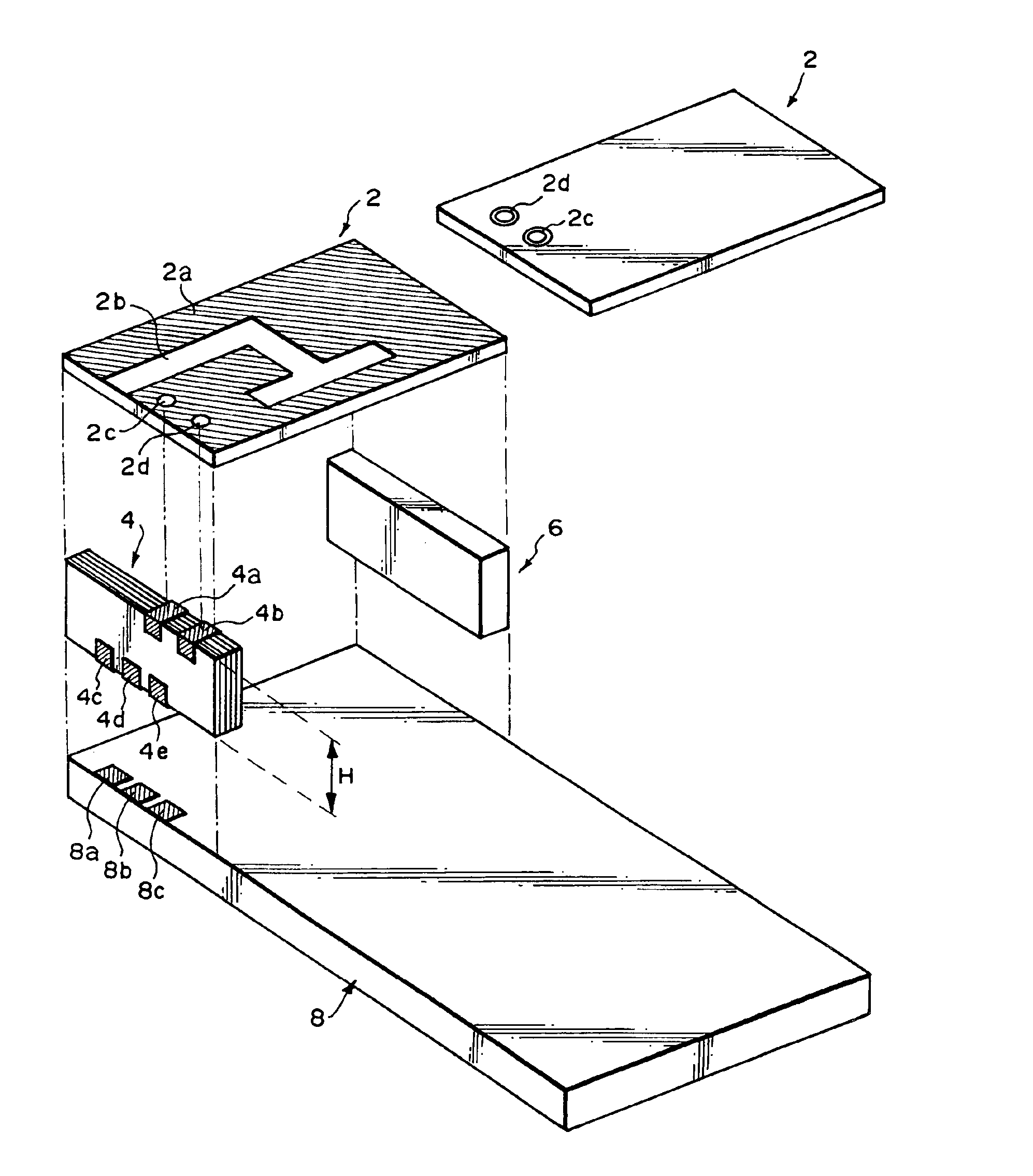
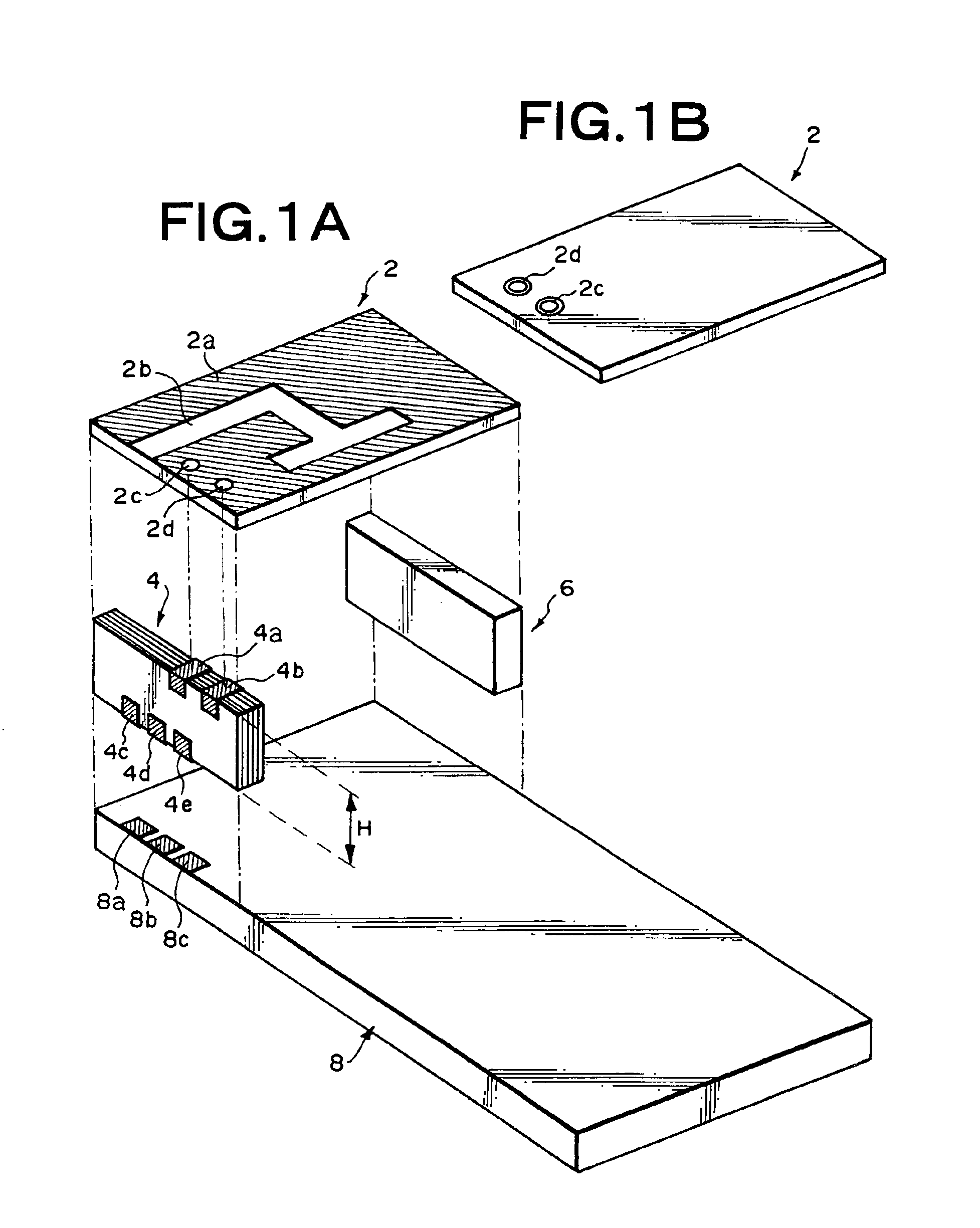
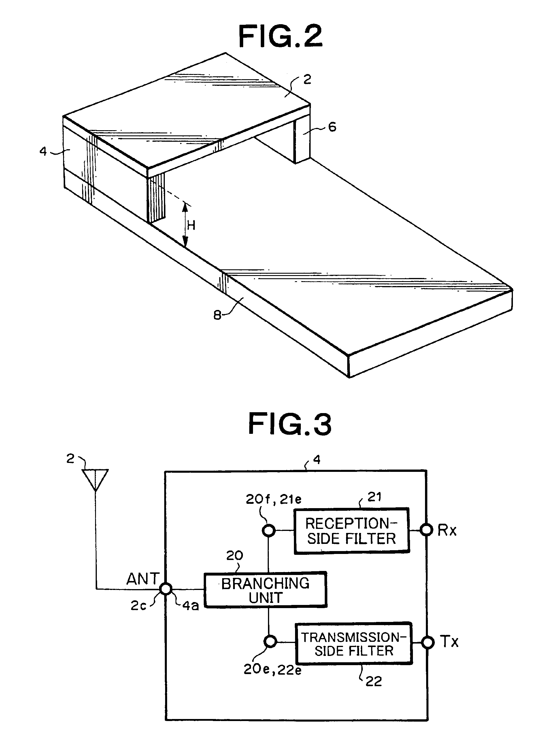
[0038]FIG. 1A is a schematic exploded perspective view showing an antenna apparatus according to the present invention, FIG. 1B is a perspective view showing a back surface of a radiation member of the antenna apparatus, and FIG. 2 is a schematic perspective view showing an assembled state of the antenna apparatus.

[0039]In FIGS. 1A and 2, a radiation member 2 is supported by two support portions 4, 6, and the support portions are attached onto a mount board or mount substrate 8.

[0040]In the radiation member 2 formed in a flat plate shape, a radiation electrode 2a is formed on one approximately rectangular surface (the upper surface in the drawing) of a substrate formed of dielectric materials such as Teflon (registered trademark) and epoxy resin. The thickness of the substrate of the radiation member 2 is not specifically limited if a desired strength of the radiation member is obtained, and is, for example, 0.1 to 2.0 mm. The dimension of the rectangular shape of the surface of the...

second embodiment

[0051]FIG. 8 is a block diagram of the laminated peripheral circuit of the antenna apparatus according to the present invention.

[0052]In the present embodiment, the peripheral circuit formed in the laminated peripheral circuit member constituting the support portion 4 is different from that of the first embodiment. That is, in the first embodiment, one frequency band is transmitted / received, but in the second embodiment, two frequency bands are transmitted / received. These two frequency bands are, for example, a frequency band of a personal communication system (PCS) in the vicinity of 2 GHz and a frequency band of an advanced mobile phone service (AMPS) in the vicinity of 900 MHz. Accordingly, the antenna apparatus can be used in a PCS / AMPS dual mode mobile phone. It is to be noted that in the present embodiment the shape of the slot 2b of the radiation member 2 is designed so that the radiation electrode 2a causes resonance in the two frequency bands.

[0053]As shown in FIG. 8, the l...

third embodiment

[0055]FIG. 10 is a block diagram of the laminated peripheral circuit of the antenna apparatus according to the present invention.

[0056]The present embodiment is different from the second embodiment in the peripheral circuit formed in the laminated peripheral circuit member constituting the support portion 4. That is, two frequency bands are transmitted / received in the second embodiment, whereas three frequency bands are transmitted / received in the third embodiment. These three frequency bands are, for example, an 800 MHz band for a global system for mobile communication (GSM), a 1.8 GHz band for a digital communication system (DCS), and a 2 GHz band for the PCS. Accordingly, an antenna apparatus is obtained for a small-sized communication apparatus which handles three frequency bands and which has a multiplicity of functions. It is to be noted that in the present embodiment, the shape of the slot 2b of the radiation member 2 is designed so that the radiation electrode 2a causes reso...


PUM


Abstract

An approximately rectangular plate-shaped radiation member (2) is provided and support portions (4,6) are attached to lower surface end portions adjacent to a pair of parallel shorter sides of the radiation member (2). The support portion (4) is composed of a laminated circuit member including a laminated demultiplexer and a laminated band pass filter of the reception side and the transmission side respectively connected to the laminated demultiplexer. The radiation member (2) has a power supply terminal (2c) and a ground terminal (2d) at the end portion where the support portion (4) is mounted. The power supply terminal (2c) and the ground terminal (2d) are connected to an antenna terminal (4a) and the ground terminal (4b) of the laminated circuit, respectively. The radiation member (2) has a radiation electrode (2a) where a slot (2b) is formed. The shape of the slot is set so that the radiation electrode (2a) causes resonance in a plurality of frequency bands.

Description

[0001]This application is a 371 of PCT / JP02 / 01531 filed on Feb. 21, 2002, published on Aug. 29, 2002 under publication number WO 02 / 067372 A1 and claims priority benefits of Japanese Patent Application No. 2001-48294 filed Feb. 23, 2001 and Japanese Patent Application No. 2001-251236 filed Aug. 22, 2001.TECHNICAL FIELD[0002]The present invention relates to a technical field of radio communication, particularly to an antenna apparatus suitable for use in mobile communication and radio local area network (LAN), into which a peripheral circuit portion is incorporated, and a communication apparatus using the antenna apparatus.BACKGROUND ART[0003]As an antenna for use in radio communication of MHz band to GHz band such as mobile communication, for example, there has heretofore been known an antenna in which a single sheet-shaped conductive member is used to constitute an antenna radiation member as described in JP(A)2000-4116. In this antenna, a ground surface spacer is disposed between ...

Claims


Application Information

Patent Timeline
Patent Type & Authority Patents(United States)
IPC IPC(8): H01Q9/04H01Q5/00H01P1/213H01Q1/38H01Q13/10H03H7/01H01Q21/30H01Q21/28H01Q1/24H03H7/46H01P1/20H01Q21/00H03H7/00H04B1/44H04B1/48H04B1/50H03H7/075
CPCH01P1/213H04B1/50H01Q1/243H01Q1/38H01Q9/0421H01Q9/0442H01Q13/10H01Q21/28H01Q21/30H03H7/0115H03H7/1766H03H7/1791H03H7/461H04B1/48H01P1/2135H03H2001/0085
Inventor FUKUDA, KOICHIICHIKAWA, HIROSHIOYAMA, RYUJIHORIE, RYOKAMEDA, SHOZABUROSUZUKI, MITSUHIRO
Owner UBE IND LTD
Why Eureka
Try Eureka