Active-type electroluminescent display

a technology of active-type electroluminescent display and display screen, which is applied in the direction of luminescent screen, discharge tube, identification means, etc., can solve the problems of increasing the severity of the problem, the intensity of the el element decreases, etc., and the intensity of the light emission decreases. , the effect of reducing the resistance of the connection conductor

Inactive Publication Date: 2005-06-28
SANYO ELECTRIC CO LTD
View PDF22 Cites 214 Cited by
  • Summary
  • Abstract
  • Description
  • Claims
  • Application Information

AI Technical Summary

Benefits of technology

[0019]In another aspect of the invention, the second electrode acts as a common electrode spreading all over the panel. Since the second electrode acting as a common electrode receives a large current, a large voltage drop fixed as the product of the conductor resistance and above large current arises so that the intensity of the light emission decreases. However, the above-mentioned multilayer structure can reduce the conductor resistance.
[0020]In yet another aspect of the present invention, the light emission element comprises an electroluminescent element in which an emissive layer is interposed between the first electrode and the second electrode. The emissive layer includes an organic compound with a luminous function. That is, the present invention is applicable to organic EL elements. In a current drive-type organic EL element, the present invention can reduce the resistance of the connection conductor which connects the cathode into which a large current is sunk and a signal supply portion

Problems solved by technology

The large resistance component of the connection conductor causes a large voltage drop, thus decreasi

Method used


Image

  • Active-type electroluminescent display
  • Active-type electroluminescent display
  • Active-type electroluminescent display

Examples


Embodiment Construction

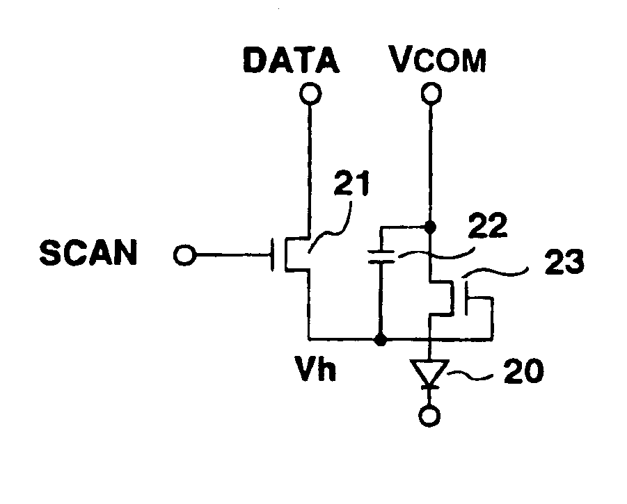
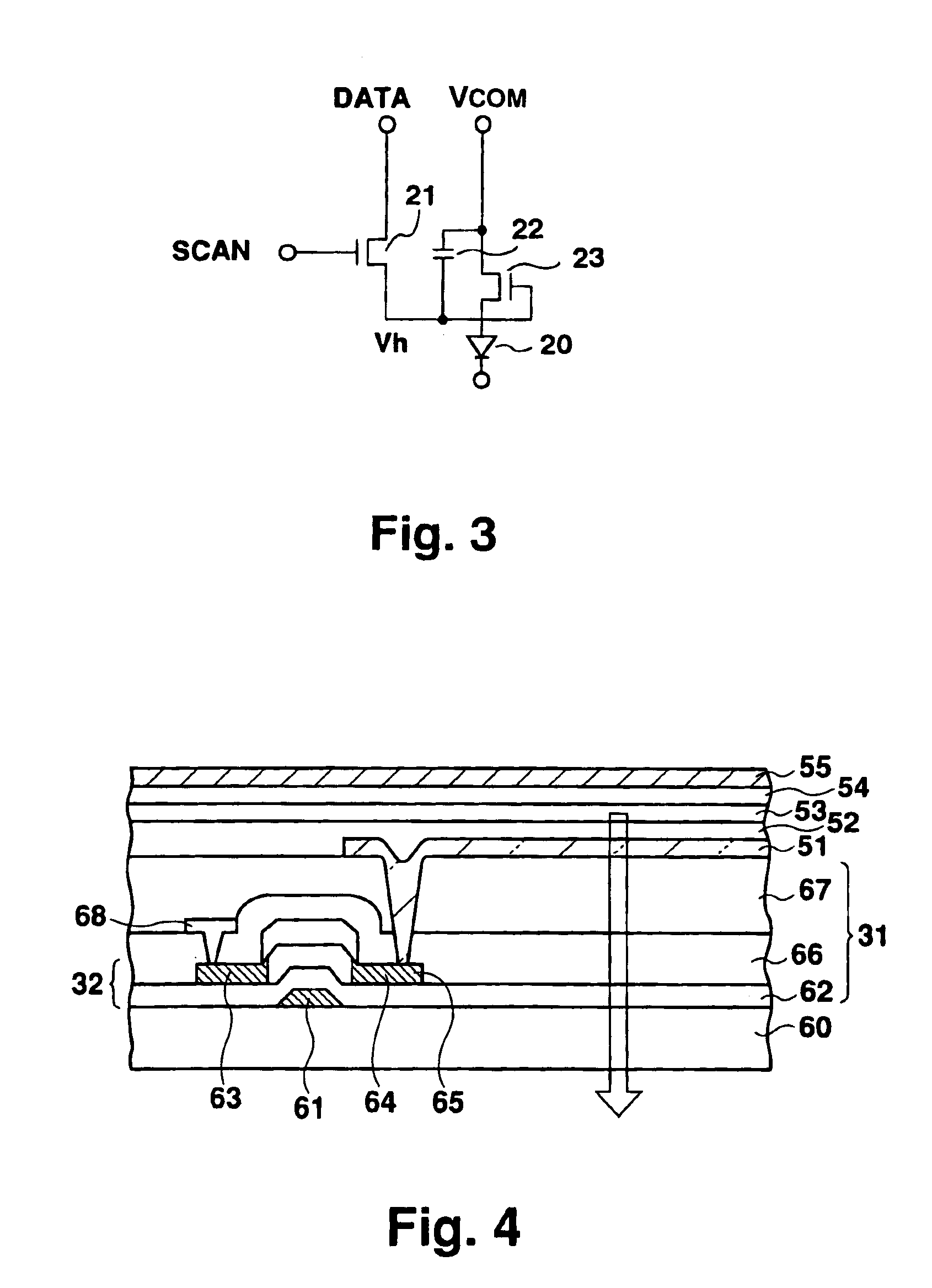
[0032]An EL display according to the present invention is an active-type EL display. The configuration of each pixel is shown in FIG. 3.

[0033]A pixel consists of an organic EL element 20, a first switching TFT 21, a capacitor 22, and a second TFT 23. The first TFT 21 is turned on / off by a selection signal Scan and a display signal Data is applied its drain. The capacitor 22 is electrically charged by the display signal Data supplied when the TFT 21 is turned on and holds the charged voltage Vh when the TFT 21 is turned off. The second TFT 23 has a drain connected to the drive power supply COM and a source connected to an anode electrode and drives the organic EL element 20 when the holding voltage vh of the capacitor 0.22 is applied to the gate.

[0034]When the TFT 21 is turned on with the selection signal Scan being at an H level during a selected horizontal scanning period (1H), the display signal Data is supplied to the capacitor 22. Thus, the capacitor 22 is charged to the voltage...


PUM


Abstract

In an active-type electroluminescent (EL) display, a conductor interconnecting a cathode (55) of an EL panel (30, 40) and a connection terminal of a signal input substrate (35) has a multilayer structure formed of a cathode material and a conductive material used in a thin-film transistor forming step. The conductor may be formed of a conductive material used in a thin film transistor forming step. A metal material for a gate electrode or drain electrode is preferably used as the conductive material. The connection conductor structure can reduce the electrical resistance of the connection conductor, thus preventing a decrease in display intensity of an EL display.

Description

BACKGROUND OF THE INVENTION[0001]1. Field of the Invention[0002]The present invention relates to an active-type display wherein luminescent elements, e.g. electroluminescent (EL) elements or fluorescent elements are driven with thin film transistors (TFTs).[0003]2. Description of Related Art[0004]Organic EL elements are self-emitting displays. The organic EL element does not require any backlight indispensable for liquid-crystal displays and is suitable for thinning the display structure. Since the viewing angle of the organic EL element is not limited, the organic EL element has been highly expected to be put to practical use as the next-generation display.[0005]In order to form an organic EL panel 1, as shown in FIG. 1, an anode electrode 3 formed of e.g. an ITO transparent electrode is formed on a transparent glass substrate 2. A hole-transport layer 5 of MTDATA (4,4′-bis(3-methylphenylphenylamino)biphenyl), an emissive layer 6 of TPD (4,4′,4″-tris(3-methylphenylphenylamino)triph...

Claims


Application Information

Patent Timeline
IPC IPC(8): G09G3/30G09F9/30H05B33/26H05B33/14H05B33/02H05B33/06H05B33/00G09G3/32H01L27/32H01L51/50H05B33/12
CPCG09G3/3225H01L27/3276G09G2300/0809H01L51/5221H01L27/3248G09G2300/0842H10K59/123H10K59/131H10K50/826H05B33/00
Inventor YOKOYAMA, RYOICHI
Owner SANYO ELECTRIC CO LTD
Why Eureka
Try Eureka