Noise checking method and apparatus

Inactive Publication Date: 2005-07-05
FUJITSU LTD
View PDF23 Cites 58 Cited by
  • Summary
  • Abstract
  • Description
  • Claims
  • Application Information

AI Technical Summary

Benefits of technology

[0038](2) Where an adjacent wiring line to a noticed wiring line has a plurality of proximate portions, a simulation is performed with regard to the individual proximate portions and the noticed wiring line to calculate noise waveforms, and the noise waveforms calculated with regard to all of the proximate portions and the signal waveform are synthesized with generation timings of the noise waveforms taken into consideration. Consequently, noise from the proximate portions can be taken into consideration to obtain a noise composite waveform without estimating the noise excessively lower than actual noise and in a short time.
[0039](3) The processing time can be reduced significantly by dividing a simulation model and executing simulations parallelly making use of a plurality of processing sections of a parallel processor or on a network.
[0040](4) When a questionable wiring line which has an influence on a noticed wiring line is moved on a display section, a noise composite waveform after the movement is displayed on the real time basis, or candidates to a damping resistance value are determined and presented and a noise composite waveform when a part corresponding to a damping resistance value is selected and added to the noticed wiring line is displayed. Consequently, a noise analysis can be facilitated, and the man-hours of a designer can be reduced to reduce the burden to the designer and the working efficiency can be further augmented.
[0041](5) When a noise waveform which has an influence on a noticed wiring line is moved on a display section, the generation timing (input delay timing) of the noise waveform can be dynamically changed on the real time basis only by a timing changing amount corresponding to the amount of movement of the noise waveform. Consequently, a delay time file need not be changed and the man-hours can be reduced significant

Problems solved by technology

It is demanded that various electronic apparatus (for example, an LSI, an MCM, a PCB and so forth) developed at present have augmented performances, higher operation speeds, reduced sizes and increased densities, and now, also functions of such apparatus have been much complicated.
In such a situation as just described, the problem of a wiring line delay is actualized as a result of the increase in speed.
However, the LSI of the CMOS type has a problem in that, because operating current which flows through an element is fluctuated by a great amount by switching of gates, power supply noise is generated and another problem in that the noise margin is decreased by a drop of the amplitude voltage.
Further, as such increase in speed and reduction in size/increase in density of an apparatus as described above proceed, crosstalk noise and reflection noise caused by impedance mismatching or by a large capacitive load are generated compositely, not only a delay problem by noise occurs, but also a malfunction may possibly occur in the circuit.
A certain wiring line is subject to electric interference by a switching operation of a signal which propagates in an adjacent wiring line, and noise, which is caused by the electric interference and is superposed on a signal propagating on the wiring line, is called crosstalk noise.
In a bus line, a plurality of signal lines are wired densely, and also when signals which propagate in the signal lines are switched simultaneously, high noise is generated.
This noise is called simultaneous switching noise.
Since generation of such various kinds of noise (reflection noise, crosstalk noise, simultaneous switching noise and power supply/ground bounce) as described above deteriorate the quality (signal integrity) of the waveform of a sign

Method used


Image

  • Noise checking method and apparatus
  • Noise checking method and apparatus
  • Noise checking method and apparatus

Examples


first embodiment

[0122][1] Description of the First Embodiment

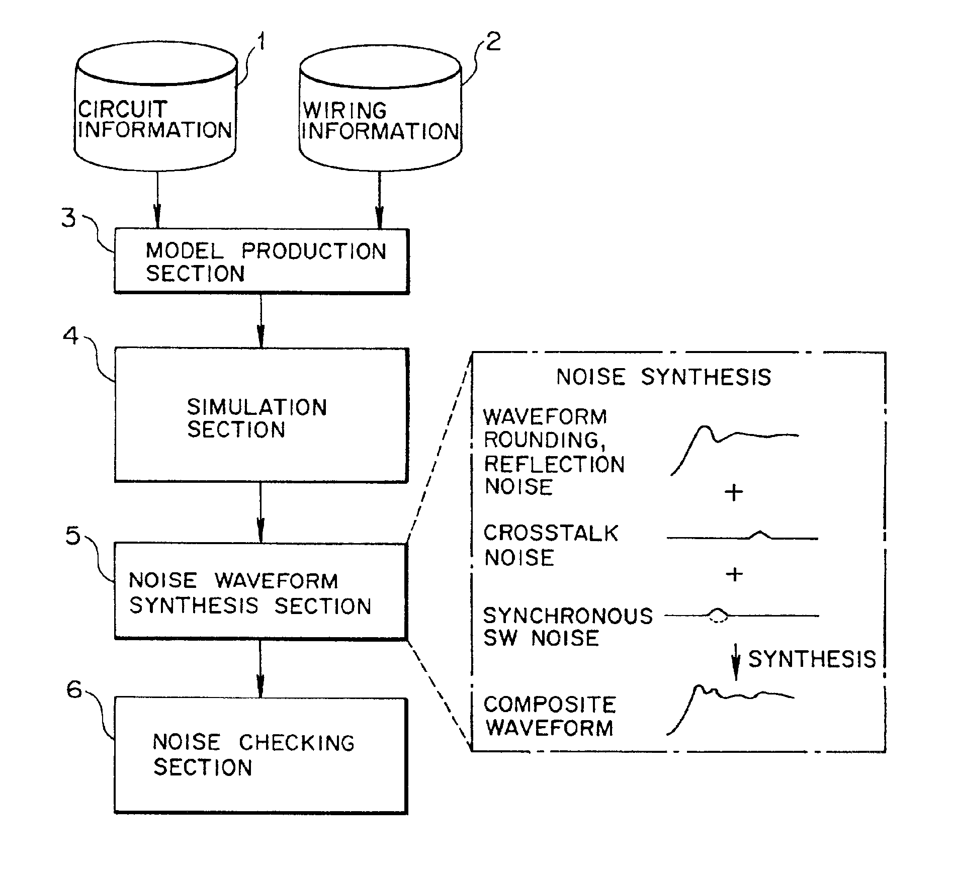
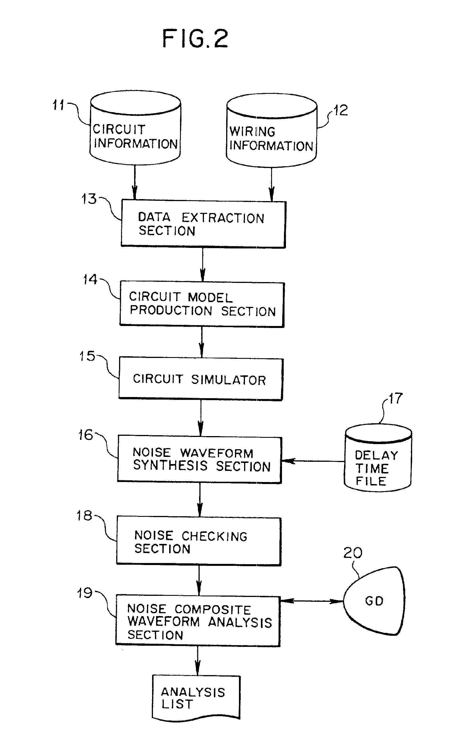
[0123]FIG. 2 is a block diagram showing a functional configuration of a noise checking apparatus as a first embodiment of the present invention. As shown in FIG. 2, the noise checking apparatus of the first embodiment is an apparatus used upon circuit designing for checking noise which has an influence on a signal waveform which propagates in a noticed wiring line (hereinafter referred to as noticed net) on a design object circuit, and includes a circuit net list database 11, a mounting database 12, a data extraction section 13, a circuit model production section 14, a circuit simulator 15, a noise waveform synthesis section 16, a delay time file 17, a noise checking section 18, a noise composite waveform analysis section 19 and a display unit 20.

[0124]The circuit net list database 11 has circuit information (a net list) of the design object circuit stored in advance therein, and the mounting database 12 has wiring information of the desi...

second embodiment

[0284][2] Description of the Second Embodiment

[0285]A noise checking apparatus as a second embodiment of the present invention is configured in a similar manner to that of the first embodiment shown in FIG. 2. Therefore, the configuration of the noise checking apparatus of the second embodiment is not shown in the accompanying drawings.

[0286]However, the noise waveform synthesis section 16 in the second embodiment calculates, when it synthesizes a signal waveform and noise waveforms obtained by the circuit simulator 15, time axis direction distributions of the maximum value and the minimum value of the signal waveform with a delay variation taken into consideration and calculates time axis direction distributions of the maximum value and the minimum value of a noise waveform with a noise generation timing distribution taken into consideration for each of different kinds of noise, and synthesizes the time axis direction distributions of the maximum value and the minimum value of the ...


PUM


Abstract

In order to achieve augmentation of the accuracy in calculation of noise and augmentation of the accuracy in a noise check which is performed, for example, when an electronic circuit is designed and further realize significant reduction of the time required for a noise check and augmentation of the operation efficiency by reduction of the man-hours of a designer in a noise analysis, a noise checking apparatus includes a model production section (3) for producing a simulation model of a circuit portion relating to a noticed wiring line, a simulation section (4) for performing a simulation using the simulation model to calculate a signal waveform which propagates in the noticed wiring line and calculate a noise waveform superposed on the signal waveform for each kind of noise, a noise waveform synthesis section (5) for synthesizing the signal waveform and the noise waveforms with generation timings of the noise waveforms taken into consideration to obtain a noise composite waveform, and a noise checking section (6) for performing noise checking based on the noise composite waveform.

Description

[0001]This application is a continuation of international application PCT / JP99 / 02093 filed on Apr. 20, 1999.TECHNICAL FIELD[0002]This invention relates to a technique applied when design an electronic circuit of, for example, an LSI (Large Scale Integration), an MCM (Multi Chip Module), a printed circuit board (PCH: Printed-Circuit Board) and so forth is designed, and more particularly to a method of and an apparatus for checking an influence of noise which can possibly be generated by an electronic circuit of a design object (for example, reflection noise, crosstalk noise, simultaneous switching noise, power supply noise, radio wave radiation noise and so forth) on a signal waveform propagated in the electronic circuit of the design object.BACKGROUND ART[0003]It is demanded that various electronic apparatus (for example, an LSI, an MCM, a PCB and so forth) developed at present have augmented performances, higher operation speeds, reduced sizes and increased densities, and now, also...

Claims


Application Information

Patent Timeline
IPC IPC(8): G06F15/18G06F17/50G06G7/62G06G7/00H04M11/04
CPCG06F17/5036G06F30/367
Inventor SATO, TOSHIROSUWA, YUJIIWAKURA, YOSHIYUKIGOTOU, KAZUNARISATO, TOSHIAKIKANEI, KAZUYOSHITOSAKA, MASAKIYAMASHITA, YASUHIRO
Owner FUJITSU LTD
Why Eureka
Try Eureka