Analog to digital converter that services voice communications

Inactive Publication Date: 2005-07-12
AVAGO TECH WIRELESS IP SINGAPORE PTE
View PDF5 Cites 15 Cited by
  • Summary
  • Abstract
  • Description
  • Claims
  • Application Information

AI Technical Summary

Benefits of technology

[0014]With the time dithering and clock reduction operations of the present invention, single modulator clock cycle resolution is maintained at the output of the time dither clock reduction circuit. Single modulator clock cycle resolution at the output of the ADC causes the modulator to better track the analog input signal. Further, by limiting the transitions of the time dither clock reduction circuit, power consumption of the ADC is reduced. Moreover, by adding time dithering, the ADC produces less output noise in the form of tones, i.e., frequencies corresponding to a fixed clock reduction operation. Reduction in output noise also lowers Electromagnetic Interference to address FCC and radio issues.

Problems solved by technology

Unexpected gaps, e.g., dropped packets, on the wireless link between supported Bluetooth devices causes degradation in the voice communication resulting in popping, static, or other unpleasant audible event.
This problem is especially troublesome with Bluetooth devices since, in some operations, the communication link will regularly drop packets that carry the voice signals.
However, if the packetized audio data stored in the input buffer is fully consumed prior to receipt of another transmission from the first Bluetooth device, it will appear to the second Bluetooth device that packetized audio data is lost (or severely delayed), and the second Bluetooth device will provided degraded audio to the serviced user.

Method used


Image

  • Analog to digital converter that services voice communications
  • Analog to digital converter that services voice communications
  • Analog to digital converter that services voice communications

Examples


first embodiment

[0043]FIG. 3A is a block diagram illustrating the electrical components of a wireless headset that includes a WLAN transceiving integrated circuit constructed according to the present invention. The wireless headset includes the WLAN transceiving integrated circuit 300 and a number of supporting components. The Radio Frequency (RF) interface for the WLAN transceiving integrated circuit 300 includes a Power Amplifier (PA) 302, a Receive / Transmit switch 304, and an antenna 306. The power supply for wireless headset is a battery 334 that couples to the WLAN transceiving integrated circuit 300 and also couples to other components of the wireless headset. The WLAN transceiving integrated circuit 300 includes a plurality of interfaces that adhere to standardized interface formats. These interfaces include an I2C interface 308 that may couple the WLAN transceiving integrated circuit 300 to an EEPROM 309. A Pulse Code Modulated (PCM) connection 310 couples the WLAN transceiving integrated c...

second embodiment

[0045]FIG. 3B is a block diagram illustrating the electrical components of a wireless headset that includes a WLAN transceiving integrated circuit constructed according to the present invention. The embodiment of FIG. 3B is similar to the embodiment of FIG. 3A except that the embodiment of FIG. 3B includes additional integration. With such integration, the PA 352 and audio CODEC 364 are on-chip and the remaining components of the WLAN transceiving integrated circuit are referred to as WLAN transceiving integrated circuit core components 351. In still another embodiment, the WLAN transceiving integrated circuit includes an on-chip local oscillator and does not require an external crystal to provide a reference oscillation 311.

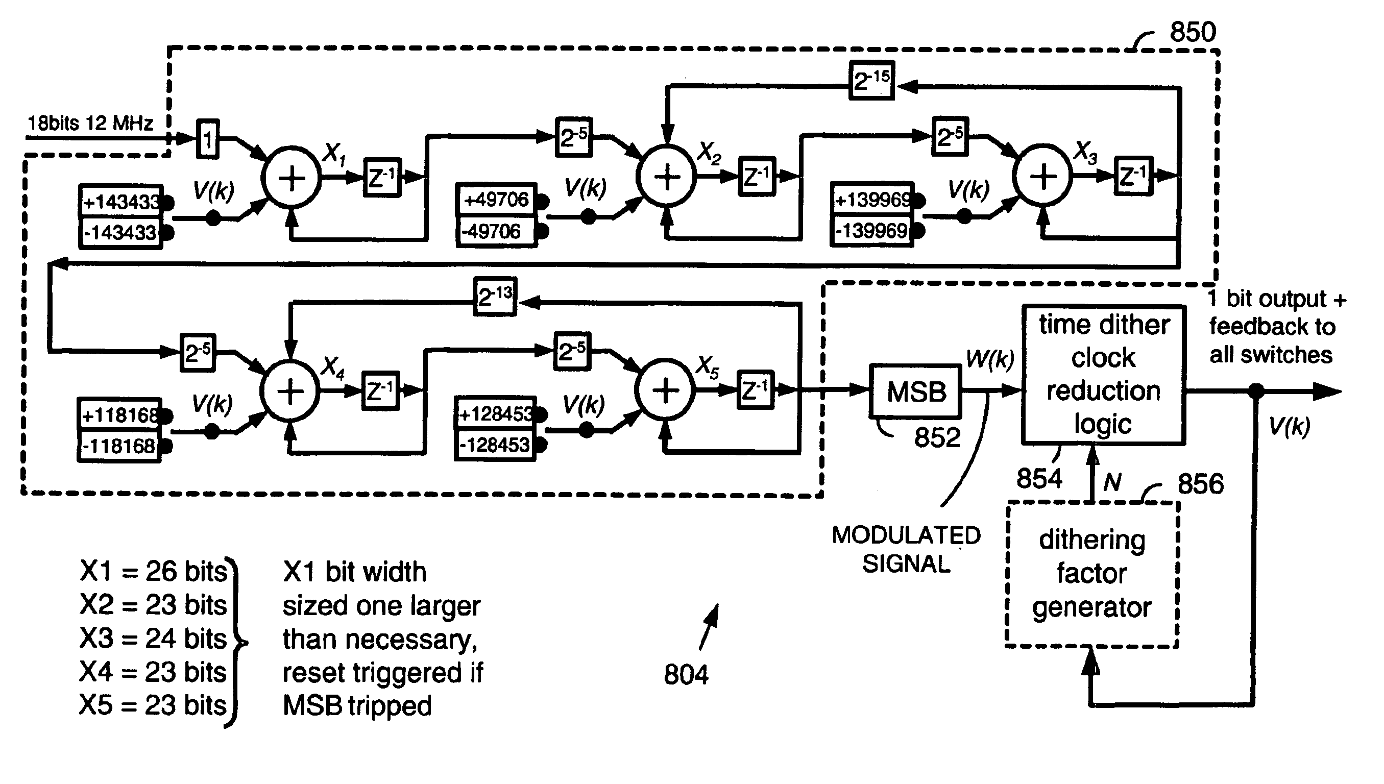
[0046]FIG. 4A is a block diagram generally illustrating the components of a WLAN transceiving integrated circuit constructed according to the present invention. The baseband processor 400 includes a radio transceiver 402, a baseband core (BBC) 404, and a PCM int...


PUM


Abstract

An Analog-to-Digital-Converter (ADC) converts an analog signal to digital data. The ADC includes a modulator, a decimation filter, and a time dither clock reduction circuit. The modulator receives the analog signal and a feedback signal and, based there upon, produces a modulated signal at a modulator clock rate. The decimation filter couples to the modulator, receives the modulated signal, and decimates and filters the modulated signal to produce the digital data. The time dither clock reduction circuit receives the modulated signal and provides the feedback signal to the modulator. The time dither clock reduction circuit applies both clock reduction and time dithering to the modulated signal to produce the feedback signal. At each modulator clock cycle, the time dithering clock reduction circuit considers modulated signals for a dithering factor, N, previous modulator clock cycles and a modulated signal for a current modulator clock cycle. If at least one constraint is satisfied for the N previous modulator clock cycles, the time dithering clock reduction circuit is allowed to transition the feedback signal with the modulated signal. If not, the time dithering clock reduction circuit holds the prior value of the feedback signal. After a transition, a new dithering factor may be determined. The ADC may be contained in a wireless local area network (WLAN) transceiving integrated circuit that services voice communications in a WLAN with at least one other WLAN device.

Description

CROSS REFERENCE TO RELATED APPLICATION[0001]This application is a continuation of and claims priority to U.S. application Ser. No. 10 / 230,692, filed Aug. 29, 2002, issued on Dec. 9, 2003 as U.S. Pat. No. 6,661,360, which claims priority to U.S. Provisional Application Ser. No. 60 / 356,323, filed Feb. 12, 2002, and to U.S. Provisional Application Ser. No. 60 / 402,855, filed Aug. 12, 2002, the disclosure of all incorporated herein by reference in their entirety.FIELD OF THE INVENTION[0002]The present invention relates to communications; and more particularly to signal conversion in wireless communication devices that service voice communications.BACKGROUND OF THE INVENTION[0003]The number and popularity of wireless communications devices in use continues to rise rapidly all over the world. Not only have cellular telephones become very popular, but Wireless Local Area Networking (WLAN) devices have also proliferated. One standard for wireless networking, which has been widely accepted, i...

Claims


Application Information

Patent Timeline
IPC IPC(8): H03M3/02H03M7/32H04L12/56H04Q7/38H04W84/12H04W88/06
CPCH03M3/336H03M7/3008H04W88/06H03M3/332H03M3/334H03M3/43H03M3/456H03M3/50H03M7/3028H03M7/304H04W84/12H03M3/3283H03M3/3287
Inventor LAMBERT, RUSSELL H.
Owner AVAGO TECH WIRELESS IP SINGAPORE PTE
Why Eureka
Try Eureka