Liquid crystal display device

a liquid crystal display and active matrix technology, applied in the direction of identification means, instruments, mechanical apparatus, etc., can solve the problems of increasing cost, increasing manufacturing steps, and reducing productivity, so as to improve productivity, reduce manufacturing steps in number, and improve performance

Inactive Publication Date: 2005-07-12
NEC LCD TECH CORP
View PDF21 Cites 18 Cited by
  • Summary
  • Abstract
  • Description
  • Claims
  • Application Information

AI Technical Summary

Benefits of technology

[0033]As a result of this, a liquid crystal display device for providing an organic insulating layer on a transistor substrate to improve performance can be manufactured by smaller manufacturing steps in number and productivity can be improved.

Problems solved by technology

As a result of this, manufacturing steps become complicated to cause an increase in cost and a decrease in productivity cannot be avoided.
This is also similar to the color filter on TFT technique or the unevenness reflection plate formation technique, and by a step for forming a color filter layer or an overcoat layer, a step for forming an unevenness layer, respectively, the manufacturing steps become complicated and the productivity decreases.

Method used


Image

  • Liquid crystal display device
  • Liquid crystal display device
  • Liquid crystal display device

Examples


first embodiment

(First Embodiment)

[0054]FIG. 5 is a schematic plan view of a display panel of a liquid crystal display device according to a first embodiment of this invention. This liquid crystal display device is an active matrix type liquid crystal display device in which an a-Si TFT acting as a switching element is provided on each one of intersections of an XY matrix.

[0055]As shown in FIG. 5, a display panel 10 is formed by filling a gap between a TFT substrate 11 and a transparent opposed substrate 12 with a liquid crystal. An a-Si TFT, a pixel electrode, a planarization layer and various lines, etc. are provided on the surface of the TFT substrate 11. A common electrode, a color filter layer and a light shield, etc. are provided on the surface of the opposed substrate 12.

[0056]A gate terminal electrode 13 or a data terminal electrode 14 is provided on the peripheral portion of the TFT substrate 11, and each of the terminals 13 and 14 is connected to an external signal processing circuit for ...

second embodiment

(Second Embodiment)

[0093]FIG. 10 is a plan view of a TFT substrate of a liquid crystal display device according to a second embodiment of this invention. The drawing shows a portion of unit pixel. This liquid crystal display device is a reflective type active matrix liquid crystal display device.

[0094]As shown in FIG. 10, an a-Si TFT 16 acting as an switching element has a drain electrode 37 formed in substantially rectangular shape in the pixel electrode formation area. This drain electrode 37 is connected to a reflection electrode 41 described below via contact through-holes 23, 35. Also, a semiconductor layer 19 is formed in correspondence with the drain electrode 37. The other configuration and action are similar to those of the TFT substrate shown in FIG. 6.

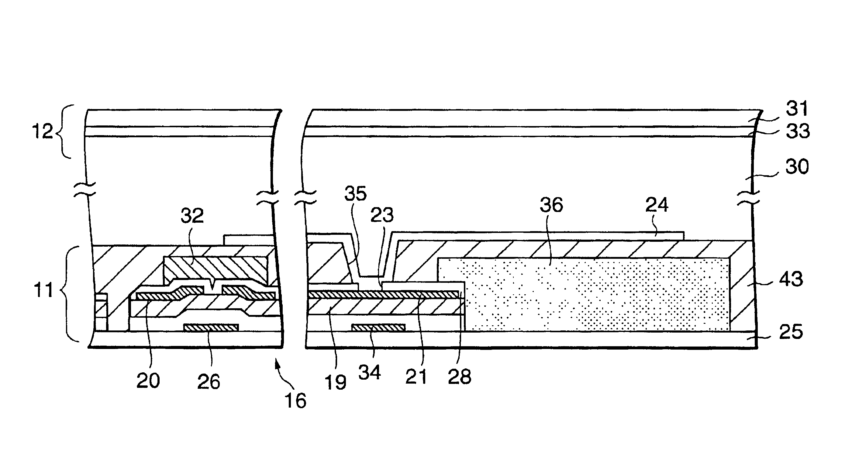
[0095]FIGS. 11A and 11B show sectional structures of each portion of FIG. 10, and FIG. 11A is a sectional view taken along line A—A, and FIG. 11B is a sectional view taken along line B—B. As shown in FIG. 11A, a gate electro...

third embodiment

(Third Embodiment)

[0106]FIG. 13 is a plan view of a TFT substrate of a liquid crystal display device according to a third embodiment of this invention. The drawing shows a portion of unit pixel. This liquid crystal display device is a reflective active matrix type liquid crystal display device.

[0107]As shown in FIG. 13, an a-Si TFT 16 acting as an switching element has a drain electrode 21 formed in L shape so that substantially half of the drain electrode overlaps with storage line 22 provided in parallel with gate line 17. Also, plural prism-shaped base posts 42 acting as bases of an unevenness layer 39 are provided. The other configuration and action are similar to those of the TFT substrate shown in FIG. 10.

[0108]FIGS. 14A and 14B show sectional structures of each portion of FIG. 13, and FIG. 14A is a sectional view taken along line A—A, and FIG. 14B is a sectional view taken along line B—B. As shown in FIG. 14A, contact through-holes 23, 35 are provided on a storage capacity el...


PUM

PropertyMeasurementUnit
thicknessaaaaaaaaaa
thicknessesaaaaaaaaaa

Abstract

There is provided a liquid crystal display device comprising a plurality of pixels arranged in a matrix form, each of the pixels including a pixel electrode formation area wherein a pixel electrode is formed and a thin film transistor formation area wherein a thin film transistor is formed and connected to the pixel electrode. The thin film transistor having a semiconductor layer serving as a channel, a terminal formed to be connected to the pixel electrode, a passivation layer formed to cover the thin film transistor and an organic insulating layer covering the passivation layer. The semiconductor layer is extended from a channel toward the pixel electrode formation area beyond the terminal and terminated in the pixel electrode formation area to form a termination end that is aligned with a termination end of the passivation layer. The organic insulating layer is elongated to cover the termination ends of the semiconductor layer and the passivation layer.

Description

BACKGROUND OF THE INVENTION[0001]1. Field of the Invention[0002]This invention relates to a liquid crystal display device, and particularly to an active matrix type liquid crystal display device.[0003]2. Description of Related Art[0004]Conventionally an amorphous silicon thin film transistor (a-Si TFT) of channel etching type has been known as a switching element for an active matrix type liquid crystal display device.[0005]FIG. 1 is a plan view of a conventional TFT array for liquid crystal display device. The drawing shows a portion of unit pixel. FIG. 2 is a sectional view of a TFT part of FIG. 1, and FIGS. 3A and 3B show terminal parts of FIG. 1 and FIG. 3A is a sectional view of a gate terminal electrode part and FIG. 3B is a sectional view of a data terminal electrode part.[0006]As shown in FIG. 1, an a-Si TFT 1 is provided every pixel of an intersection of an XY matrix, and has a gate electrode 2, a source electrode 3 and a drain electrode 4 oppositely placed over the gate el...

Claims


Application Information

Patent Timeline
Patent Type & Authority Patents(United States)
IPC IPC(8): G02F1/13G02F1/1362G02F1/1335G02F1/136G02F1/1368G09F9/30H01L21/336H01L29/786
CPCG02F1/136227G02F1/136286G02F2001/136236G02F2001/13629G02F2202/10G02F1/136236G02F1/13629E04H17/16E04H17/20F16B2200/81
Inventor SAKAMOTO, MICHIAKIYAMAGUCHI, YUICHI
Owner NEC LCD TECH CORP
Why Eureka
Try Eureka