Wavelength converting element and method of manufacture thereof

Inactive Publication Date: 2005-07-12
FUJIFILM CORP +1
View PDF12 Cites 3 Cited by
  • Summary
  • Abstract
  • Description
  • Claims
  • Application Information

AI Technical Summary

Benefits of technology

[0022]On the other hand, in the method for manufacturing a wavelength converting element relating to the present invention, in the process for forming the waveguide, the waveguide can be fabricated by using a negative photoresist of a film thickness which is relatively thin, and highly accurat

Problems solved by technology

Even if a waveguide is formed at the surface thereof, the joining with the TE mode is poor.
Thus, it is difficult to efficiently join a semiconductor laser.
Thus, there are problems in that the inverted domains are only formed at a shallow position with respect to the waveguide such that there is little overlapping of the fundamental wave and the inverted domain portion, and the waveguide converting efficiency i

Method used


Image

  • Wavelength converting element and method of manufacture thereof
  • Wavelength converting element and method of manufacture thereof
  • Wavelength converting element and method of manufacture thereof

Examples


Embodiment Construction

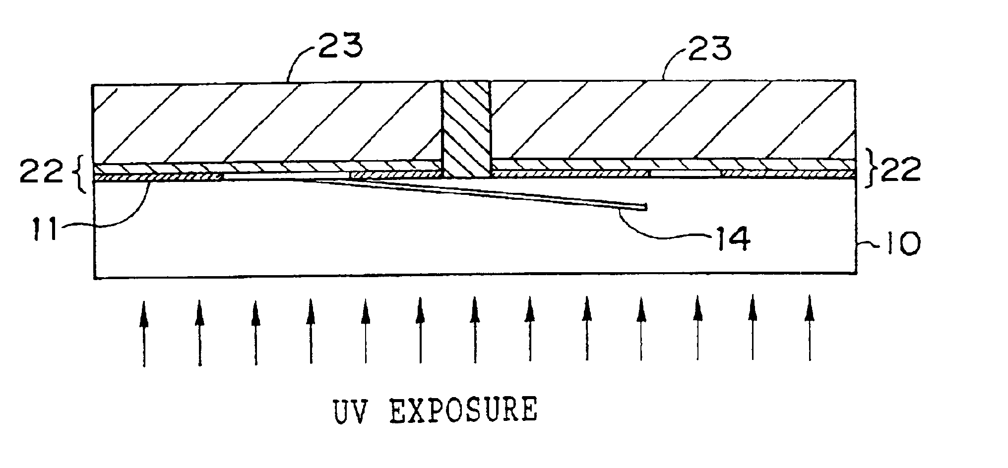
[0036]An embodiment of the present invention will be described in detail hereinafter with reference to the figures.

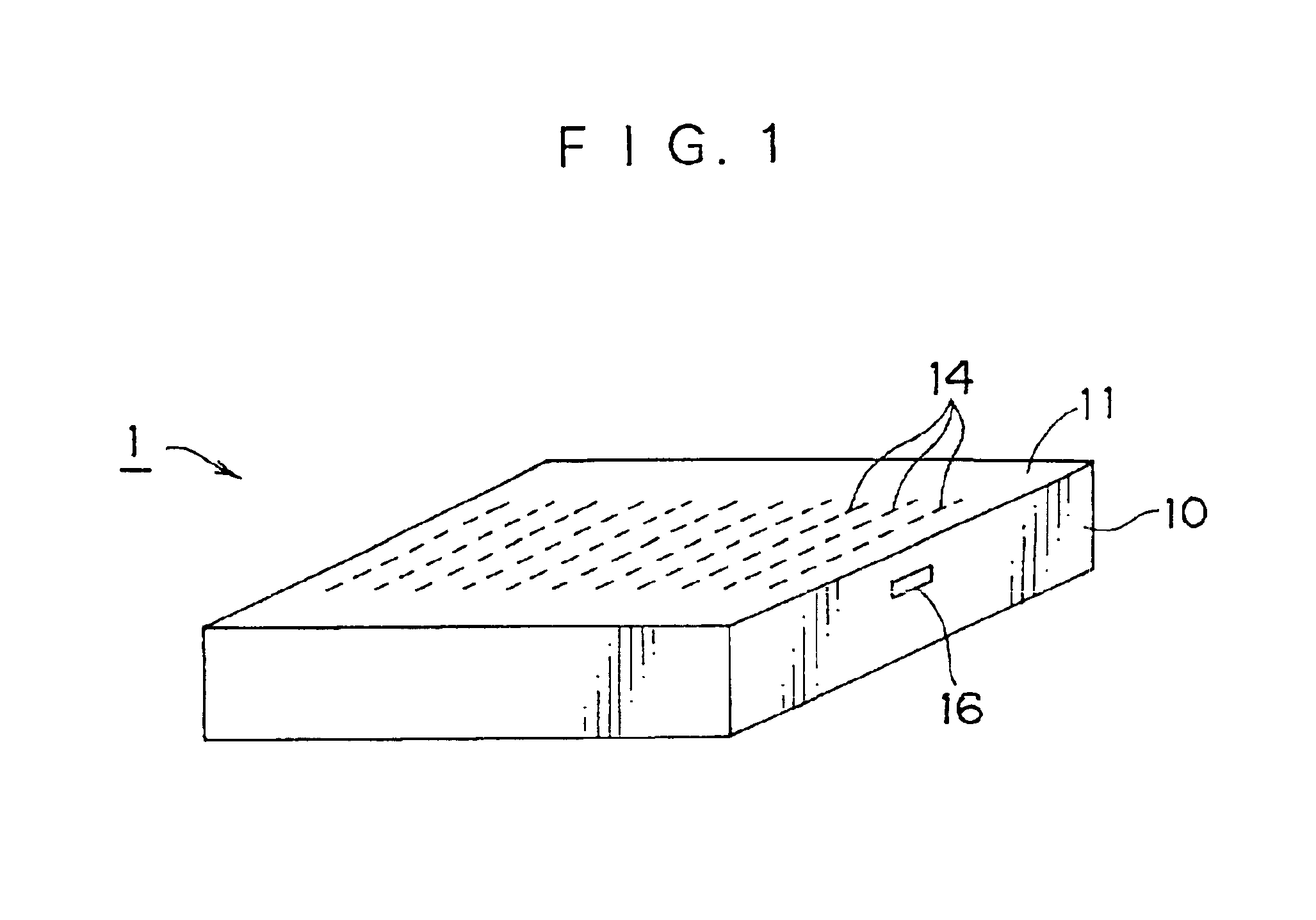
[0037]As shown in FIG. 1, a wavelength converting element 1 relating to the embodiment of the present invention has a plurality of inverted domains 14 which are formed at predetermined intervals at the interior of an optical crystal substrate 10, and a waveguide 16 formed in a direction orthogonal to the respective inverted domains 14.

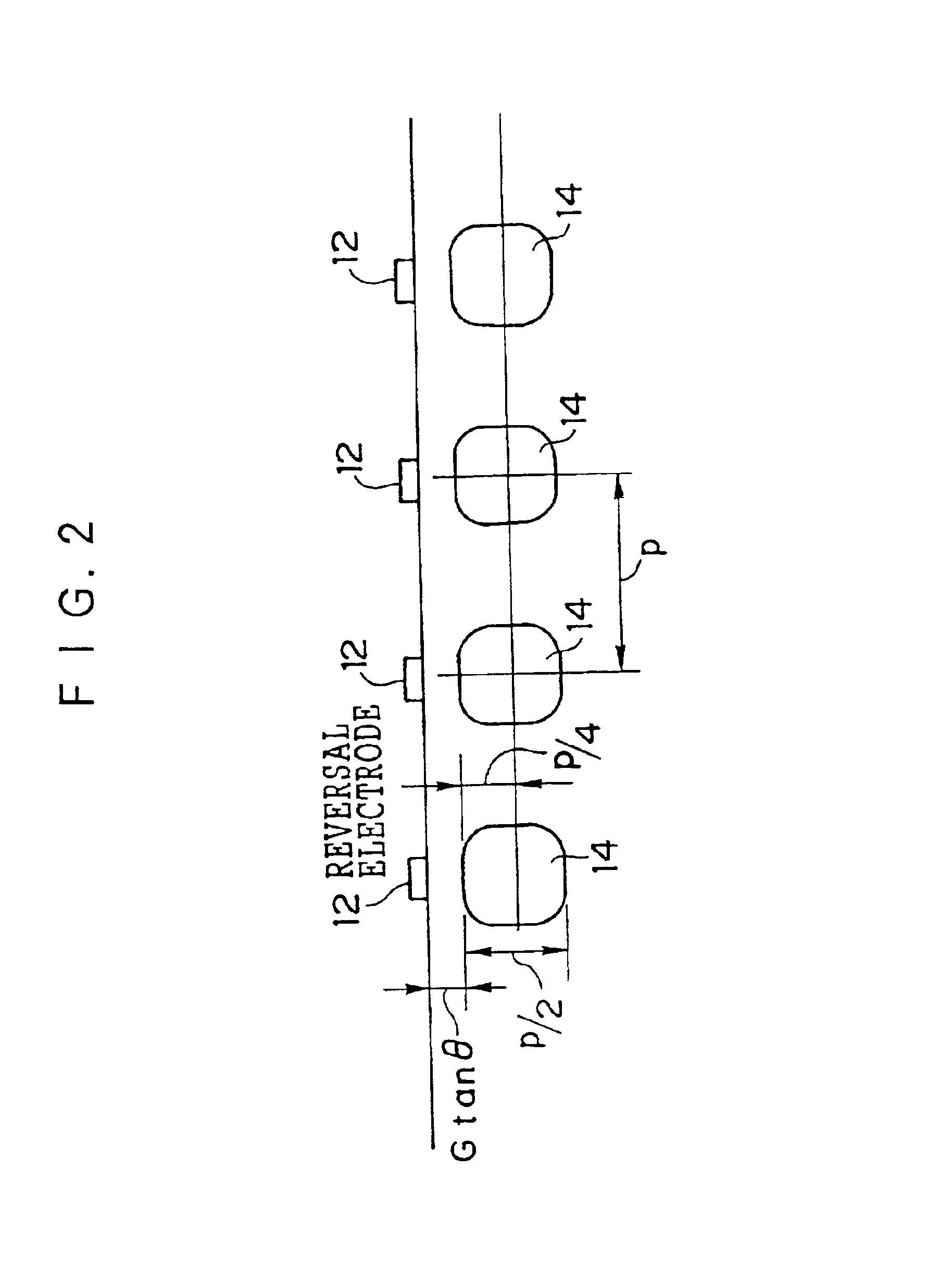
[0038]FIG. 2 is a sectional view of the wavelength converting element 1 shown in FIG. 1, as viewed from the Y axis direction. Comb-shaped reversal electrodes 12 are formed at a main surface 11 of the optical crystal substrate 10. A pitch p between the respective reversal electrodes 12 can be computed from the phase matching wavelength of the second harmonic and the fundamental wave. When the pitch p is determined, the size of the region which optimizes the efficiency of the inverted domains 14 is determined. Usually, the size of the region...


PUM


Abstract

A wavelength converting element is provided in which a fundamental wave with respect to an optical crystal substrate and a peak of a vertical transverse mode of a second harmonic are made to coincide, the converting efficiency is good, and a beam shape which enables good joining to a lens or an optical fiber is obtained. Given that an angle formed by a surface of the optical crystal substrate and a C axis of the optical crystal substrate is θ, a period at which inverted domains are formed is p, and a distance from a distal end of a comb-shaped electrode for forming the inverted domain to a central position of a waveguide is G, in the ion implantation, a concentration peak of the ion implantation is formed at a distance of substantially (G·tanθ+p/4) from the surface of the optical crystal substrate.

Description

BACKGROUND OF THE INVENTION[0001]1. Field of the Invention[0002]The present invention relates to a wavelength converting element and a method of manufacture thereof, and in particular, to a wavelength converting element in which the peak of a vertical transverse mode with respect to a substrate of a second harmonic is made to coincide with a fundamental wave such that an improvement in the wavelength converting efficiency and an improvement in the beam shape are achieved, and to a method of manufacturing the wavelength converting element.[0003]2. Description of the Related Art[0004]Wavelength converting elements have been conventionally manufactured which wavelength-convert a fundamental wave into a second harmonic by using an element provided with a region (inverted domains) at which spontaneous polarization of a ferroelectric having a non-linear optical effect, e.g., a crystal such as LiNbO3 or LiTaO3, is periodically inverted.[0005]The inverted domains used here have the feature ...

Claims


Application Information

Patent Timeline
IPC IPC(8): G02B6/13G02F1/377G02B6/134G02F1/35G02F1/03G02F1/01
CPCG02B6/1347G02F1/3775G02F1/0316G02F2201/066
Inventor TSURUMA, ISAO
Owner FUJIFILM CORP
Why Eureka
Try Eureka