Bonded member comprising different materials, and production method thereof

a technology of bonded members and composite bonded components, which is applied in the direction of manufacturing tools, welding/cutting media/materials, and manufacturing tools, etc., can solve the problems of deteriorating product reliability, unfavorable increase in production costs of these composite bonded members, and inability to achieve desired bonding strength and air tightness in some cases, and achieves simple operation

Inactive Publication Date: 2005-07-19
NGK INSULATORS LTD
View PDF11 Cites 78 Cited by
  • Summary
  • Abstract
  • Description
  • Claims
  • Application Information

AI Technical Summary

Benefits of technology

[0014]The present invention has been conceived in view of such problems of the prior art. An object of the present invention is to provide a bonded member comprising different materials which are bonded together, the bonded member having air tightness at the interface between the bonded materials and also having thermal cycle properties and thermal shock properties and being able to be produced by a simple operation, and an easy-to-practice production method of the bonded member comprising different materials.

Problems solved by technology

However, during a cooling process after high-temperature bonding, thermal stress caused by a difference in thermal expansion coefficient between the different materials or between the solder material used for bonding the different materials together and the materials occurs, thereby causing separation at the interface between the materials or causing cracks in the vicinity of the interface if one of the materials is brittle, so that desired bonding strength and air tightness cannot be obtained in some cases.
Since products having the aforementioned troubles broken during a production process must be discarded as defective products, this results in an unfavorable increase in production costs of these composite bonded members.
Further, if the product is subjected to thermal cycles in use, these troubles occur after use for a certain time period to cause a deterioration in the reliability of the product.
Meanwhile, in these methods, unless some measures are taken against thermal stress, which occurs at the interface between bonded materials, so as to reduce the thermal stress, cracks are often formed in a base material which is vulnerable to the thermal stress or separation occurs at the interface, so that bonding strength as well as various properties required from a composite bonded member such as air tightness may be influenced.
Particularly, it is very difficult to bond a low-strength base material such as aluminum nitride and a member composed of metal or the like to each other without the occurrence of the above problems.
However, in a case where a solder material comprising Ag or Cu is used, they may be difficult to use in some cases due to a problem caused by oxidation of the solder material when a composite member obtained is exposed to an application environment of 400° C. or higher under an oxidizing atmosphere, a problem of evaporation of the solder material which is caused by a high vapor pressure when the composite member is used at a high temperature and a low pressure, a problem of migration when the composite member is energized upon use, and a problem of a reaction with an Mo oxide.
As a result, the base material is cracked by a thermal cycle and thermal shock.
Accordingly, durability when the bonded interface is exposed to a thermal cycle and thermal shock lowers and the bonded interface deteriorates rapidly, so that there arises a problem that equipment and apparatus having such a bonded interface are liable to be impossible to use.
However, these metals are vigorously oxidized at high temperatures in the air.
Therefore, they are not suitable for use as metal materials for members whose exposure to a high temperature atmosphere is imaginable, such as a feeding terminal for a susceptor and a metal ring for attaching the susceptor to a chamber (hereinafter simply referred to as “chamber”) for producing a semiconductor.
However, the foregoing bonding structure has such problems that the number of parts is large and that since deterioration of the metallic member 17 occurs due to its oxidation if the atmosphere protector 9 and the metallic member 17 are not fully bonded to each other, a very high production control ability is required.
However, since a Cu-based solder material is used, usable temperatures are limited due to the forgoing problem caused by oxidation of the solder material and the foregoing problem of evaporation of the solder material which is caused by a high vapor pressure.
However, in the solid-phase bonding adopted in the production method of a composite member which is proposed in the foregoing specification, a pressing operation and other operations are required, and it is imaginable that procedures of the operations may be complicated in some cases.
Hence, the method is susceptible to further improvements.

Method used


Image

  • Bonded member comprising different materials, and production method thereof
  • Bonded member comprising different materials, and production method thereof
  • Bonded member comprising different materials, and production method thereof

Examples


examples

[0095]Hereinafter, examples of the present invention will be described. However, it is needless to say that the present invention shall not be limited to the following examples.

examples 1 to 8

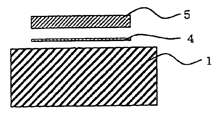
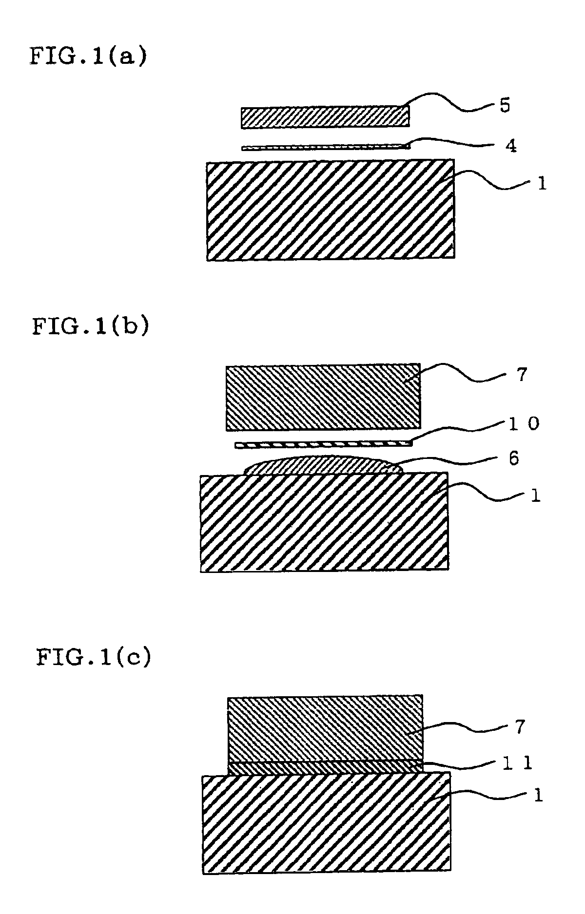
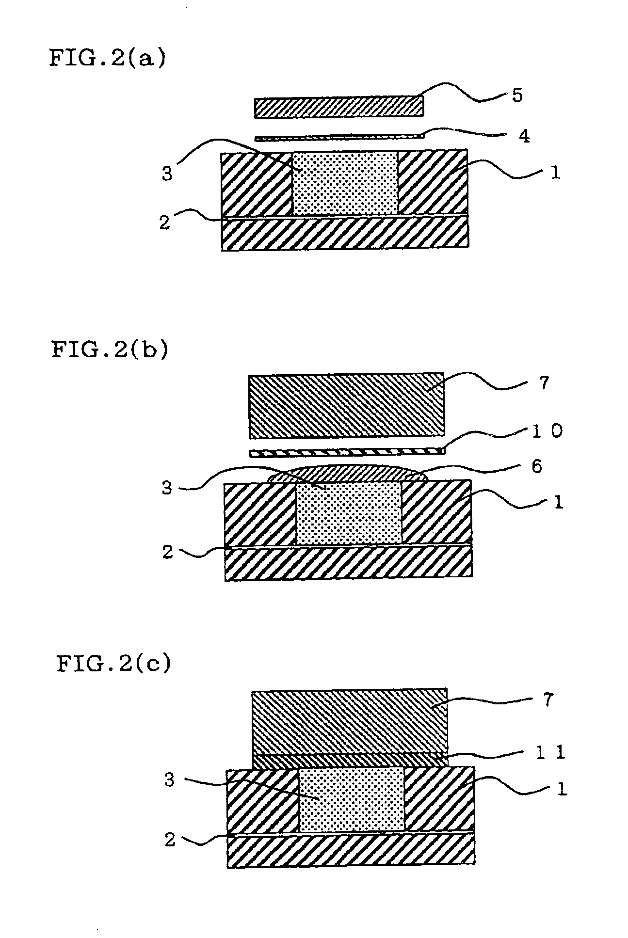
[0096]On the surface of a base material made of AlN, a Ti foil having a diameter of 6.5 mm and a thickness of 5 μm (weight: about 0.75 mg) was disposed, and on the Ti foil, a pure Au solder material having a diameter of 6.5 mm and a thickness of 600 μm (weight: about 385 mg) was disposed. Then, they were heated in a vacuum atmosphere at 1,100° C. for 10 minutes, thereby forming a 600-μm-thick Au precoat layer including a layer of a reaction product of the active metal on the base material. For adjustment of the thickness of the precoat layer, the heat treatment was carried out with setting up a simple weir made of carbon around the pure Au solder material. On the precoat layer, an Al foil having a diameter of 5 mm and a thickness of 13 μm (weight: about 0.7 mg) was disposed as an insertion metal layer, and then an Ni or Kovar terminal (diameter: 5 mm) was disposed thereon as a metallic member (terminal). Then, they were heat-pressed in a vacuum atmosphere at 600 to 900° C. for 10 or...

examples 9 to 11

[0097]The procedure for the foregoing Examples 1 to 8 was repeated except that in place of the Al foil serving as the insertion metal layer, a crushed Au-5Al alloy or Au-3Al alloy was disposed on the precoat layer in an amount of about 32 mg (corresponds to a diameter of 6.5 mm and a thickness of 50 μm at the time of melting upon preparation of these alloys), that an Ni terminal (diameter: 5 mm) was used as the metallic member (terminal), and that bonding was carried out at 700° C. or 800° C. Thereby, bonded members comprising different materials were obtained (Examples 9 to 11). In all cases, no cracks were formed in the base materials at the time of bonding.


PUM

PropertyMeasurementUnit
temperatureaaaaaaaaaa
thicknessaaaaaaaaaa
melting pointaaaaaaaaaa

Abstract

A bonded member including a ceramic base material 1 and a metallic member 7 which are bonded together, wherein a solder material 5 comprising Au is disposed on the surface of the ceramic base material 1 via an active metal layer, the active metal layer and the solder material 5 are molten by heating so as to form a precoat layer 6, the metallic member 7 is disposed on the surface of the precoat layer 6 via an insertion metal layer comprising pure metal which may form an alloy having a lower melting point than Au with Au or an alloy of the pure metal and Au, and the insertion metal layer and at least a portion in the vicinity of the interface between the insertion metal layer and the precoat layer 6 are molten by heating to bond the metallic member 7 and the precoat layer 6.

Description

BACKGROUND OF THE INVENTION[0001]1. Field of the Invention[0002]The present invention relates to a bonded member comprising a ceramic base material and a metallic member which are bonded to each other, and a method for producing the bonded member.[0003]2. Description of the Related Art[0004]As a method of bonding different materials such as a ceramic base material and a metallic member to each other, a method such as one using a solder material can be used. However, during a cooling process after high-temperature bonding, thermal stress caused by a difference in thermal expansion coefficient between the different materials or between the solder material used for bonding the different materials together and the materials occurs, thereby causing separation at the interface between the materials or causing cracks in the vicinity of the interface if one of the materials is brittle, so that desired bonding strength and air tightness cannot be obtained in some cases. Since products having...

Claims


Application Information

Patent Timeline
Patent Type & Authority Patents(United States)
IPC IPC(8): B23K1/00B23K1/20B23K1/19B23K35/30B23K35/00H01R4/02B23K103/18C04B37/02C22C5/02
CPCB23K1/0008B23K1/19B23K1/20B23K35/004B23K35/3013B32B18/00C04B37/026C04B35/645B32B2309/022B32B2311/04B32B2311/18B32B2311/22B32B2311/24C04B2235/96C04B2235/9607C04B2237/125C04B2237/405H01R4/02C04B2235/6567C04B2235/6581C04B2237/121C04B2237/122C04B2237/126C04B2237/366C04B2237/406C04B2237/55C04B2237/64C04B2237/68C04B2237/704C04B2237/708C04B2237/72C04B2237/765C04B2237/84C04B2237/86B23K31/02
Inventor SHINKAI, MASAYUKIISHIKAWA, TAKAHIROKIDA, MASAHIROOHTA, MITSURU
Owner NGK INSULATORS LTD
Why Eureka
Try Eureka