Regulated growth method for laser irradiating silicon films

a technology of laser irradiation and growth method, which is applied in the direction of crystal growth process, polycrystalline material growth, chemistry apparatus and processes, etc., can solve the problems of increasing process cost, neighboring tfts with different performance parameters, etc., and achieves enhanced lateral growth length, reduced surface ridges, and reduced surface ridges

Inactive Publication Date: 2005-07-26
SHARP LAB OF AMERICA INC
View PDF6 Cites 3 Cited by
  • Summary
  • Abstract
  • Description
  • Claims
  • Application Information

AI Technical Summary

Benefits of technology

[0012]The present invention is a method that results in reduction of the surface ridges on laterally crystallized silicon films and / or the enhancement of the lateral growth length. Depending upon the operating conditions, the method can be applied to reduce the surface ridges, increase the lateral growth length, or achieve a compromise between the two. The method utilizes the temporal separation of laser pulses to achieve remelting and planarization of the surface of silicon films or, alternatively, provides additional thermal energy to the molten silicon film to prolong lateral growth.

Problems solved by technology

Even more undesirable is the formation of neighboring TFTs with different performance parameters, resulting from the random formation of TFT channels with ridges adjacent TFT channels without ridges.
This alignment process introduces additional processing steps, hence increases the cost of the process.

Method used


Image

  • Regulated growth method for laser irradiating silicon films
  • Regulated growth method for laser irradiating silicon films
  • Regulated growth method for laser irradiating silicon films

Examples


example 1

Maximum Surface Planarization

[0033]FIG. 6 illustrates a temporal beam profile at the output of the pulse extender designed to maximize surface flatness. Two pulses are shown in this case, but in principle more pulses could be generated, if so desired. The second pulse (second, in a temporal sense) has a lower intensity than the first, and it is well-separated from the first pulse. That is, the temporal separation between the two pulses is greater than the pulse duration of either pulse, with the pulse duration measured at the Full-Width-Half-Maximum (FWHM) of the pulse. Typical ranges for the various properties of the pulses are shown in FIG. 6. Typically, the pulse duration of either (both) pulses is in the range of 20-50 ns, however, longer pulses may be desirable for larger intensity pulses, measured at FHWM. The temporal separation between pulses is in the range of 60-250 ns, although wider ranges may be useful. The relative intensity reduction between pulse n and pulse n+1 is i...

example 2

Maximum Lateral Growth Length

[0034]FIG. 7 illustrates the temporal beam profile at the exit of the pulse extender designed to maximize lateral growth length. Again two pulses are shown, but in principle more pulses could be generated. An important element of this process is to make the second pulse (or other subsequent pulses) of a similar intensity to the first pulse. Further, the temporal separation between the two pulses is less than the pulse duration of either, with the pulse duration measured at the FWHM of the pulse. Typical ranges for the various properties of the pulses are shown in FIG. 7. The pulse duration (for either pulse) is in the range of 20-100 ns, measured at the FWHM. The temporal separation between pulses is in the range of 30-500 ns. The relative intensity between pulse n and pulse n+1 is approximately the same. In other words, the intensity of the subsequent pulse is similar to its predecessor.

example 3

Comprise Between Planarization and Lateral Growth Length

[0035]FIG. 8 illustrates the temporal beam profile at the exit of the pulse extender designed to compromise between the goals of surface flatness and lateral growth length. Two pulses are shown, but the invention is not limited to any particular number of pulses. To achieve a reasonable compromise between these goals, the temporal pulse separation is not too large and the pulse intensity is not too similar. Typical ranges for the various properties of the pulses are shown in FIG. 8. The pulse duration (for either pulse) is 20-50 ns, measured at the FWHM, the temporal separation between pulses is 30-150 ns, and the relative intensity is reduced in the range of 10%-50% between pulse n and pulse n+1. In other words, the intensity of the subsequent pulse is 50-90% that of its predecessor.

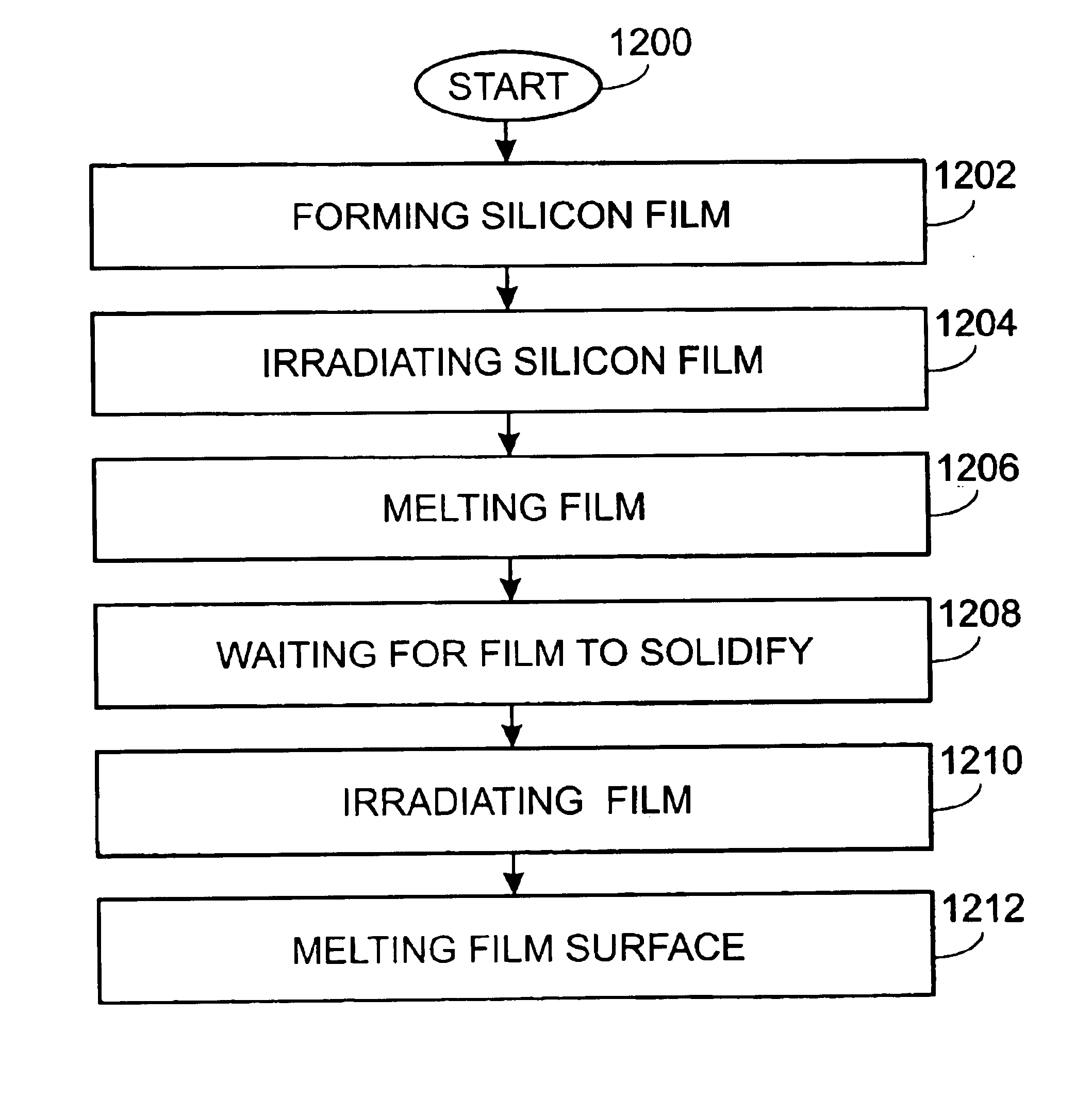
[0036]FIG. 9 is a flowchart illustrating the present invention method for maintaining a planar surface as crystal grains are laterally grown in th...


PUM

PropertyMeasurementUnit
laser wavelengthaaaaaaaaaa
widthaaaaaaaaaa
lengthaaaaaaaaaa

Abstract

A method is provided for maintaining a planar surface as crystal grains are laterally grown in the fabrication of crystallized silicon films. The method comprises: forming a film of amorphous silicon with a surface and a plurality of areas; irradiating each adjacent areas of the silicon film with a first sequence of laser pulses; and, in response to the first sequence of laser pulses, controlling the planarization of the silicon film surface between adjacent areas of the silicon film as the crystal grains are laterally grown. By controlling the number of laser pulses in the sequence, the temporal separation between pulses, and the relative intensity of the pulses, the lateral growth length characteristics of the crystal grains can be traded against the silicon film flatness. A silicon film formed by a pulsed laser sequence crystallization process is also provided.

Description

CROSS REFERENCE TO RELATED APPLICATION[0001]This application is a continuation of application Ser. No. 09 / 894,940, filed Jun. 28, 2061now U.S. Pat No. 6,648,464, entitied “System and Method for Regulating Lateral Growth in Laser Irradiated Silicon Films,” invented by Apostolos Voutsas.BACKGROUND OF THE INVENTION[0002]1. Field of the Invention[0003]This invention generally relates to liquid crystal display (LCD) and integrated circuit (IC) fabrication and, more particularly, to a silicon film and fabrication process to laser irradiate silicon film in making polycrystalline silicon thin film transistors (TFTs) for Active Matrix (AM) LCDs.[0004]2. Description of the Related Art[0005]Lateral crystallization by excimer-laser anneal (LC-ELA) is a desirable method for forming high quality polycrystalline silicon films having large and uniform grains. Further, this process permits precise control of the grain boundary locations.[0006]FIGS. 1a through 1d illustrate steps in an LC-ELA anneali...

Claims


Application Information

Patent Timeline
Patent Type & Authority Patents(United States)
IPC IPC(8): C30B1/00C30B1/02H01L21/20H01L21/336H01L29/786
CPCC30B1/023C30B29/06Y10S117/903
Inventor VOUTSAS, APOSTOLOS
Owner SHARP LAB OF AMERICA INC
Why Eureka
Try Eureka