Nonvolatile semiconductor memory device allowing high speed data transfer

a nonvolatile, data transfer technology, applied in static storage, digital storage, instruments, etc., can solve the problems of affecting the correct programming of data, increasing current consumption, affecting the correct data reading, etc., to achieve efficient data writing and reading

Active Publication Date: 2005-07-26
RENESAS ELECTRONICS CORP
View PDF4 Cites 47 Cited by
  • Summary
  • Abstract
  • Description
  • Claims
  • Application Information

AI Technical Summary

Benefits of technology

[0036]It is an object of the present invention to provide a semiconductor memory device capable of efficiently performing writing and reading of data.
[0037]It is another object of the present invention to provide a semiconductor memory device excellent in data transfer efficiency.
[0038]It is still another object of the present invention to provide a nonvolatile semiconductor memory device capable of configuring a processing system excellent in data processing efficiency.
[0042]A local bus is provided in correspondence to a memory block and a data transfer bus is commonly provided to a plurality of memory blocks. Therefore, when data writing or data reading is performed on one memory block, data to which an access is made can be transferred to another block through the data transfer bus, thereby allowing saving and back-up of data with ease. Furthermore, where a bank configuration is employed, by performing data transfer between banks, and by reading transfer data from one bank while writing is performed to another bank, a processing efficiency can be improved.
[0043]Furthermore, by performing data writing / reading individually in each of the plurality of memory blocks, data writing and reading can be simultaneously performed in memory blocks, a data bit width can be widened, and a band width of transfer data can be expanded, thereby improving a processing efficiency.

Problems solved by technology

In such a case, an amount of electrons injected into the insulating film (nitride film) of the memory cell of interest becomes insufficient, thereby impeding correct programming of data.
While it can be considered that a programming period is extended for reliable programming, current flows in a bit line in a floating state in this case, which would increase current consumption.
If storage data in the memory cell of interest is data corresponding to a programmed (write) state, a possibility arises that a erroneous determination is made that the memory cell is in an erased state, to impede a correct data reading.
Therefore, in one memory block, programming / data reading can be performed only on one memory cell, thereby impeding high-speed data writing / reading.
There arises a problem that a processing system efficiently performing a processing is difficult because of a small read data bit width and accordingly a small data band width.
Therefore, a cycle time for data writing determines an access time of the semiconductor memory device, which impedes a high speed access.

Method used


Image

  • Nonvolatile semiconductor memory device allowing high speed data transfer
  • Nonvolatile semiconductor memory device allowing high speed data transfer
  • Nonvolatile semiconductor memory device allowing high speed data transfer

Examples


first embodiment

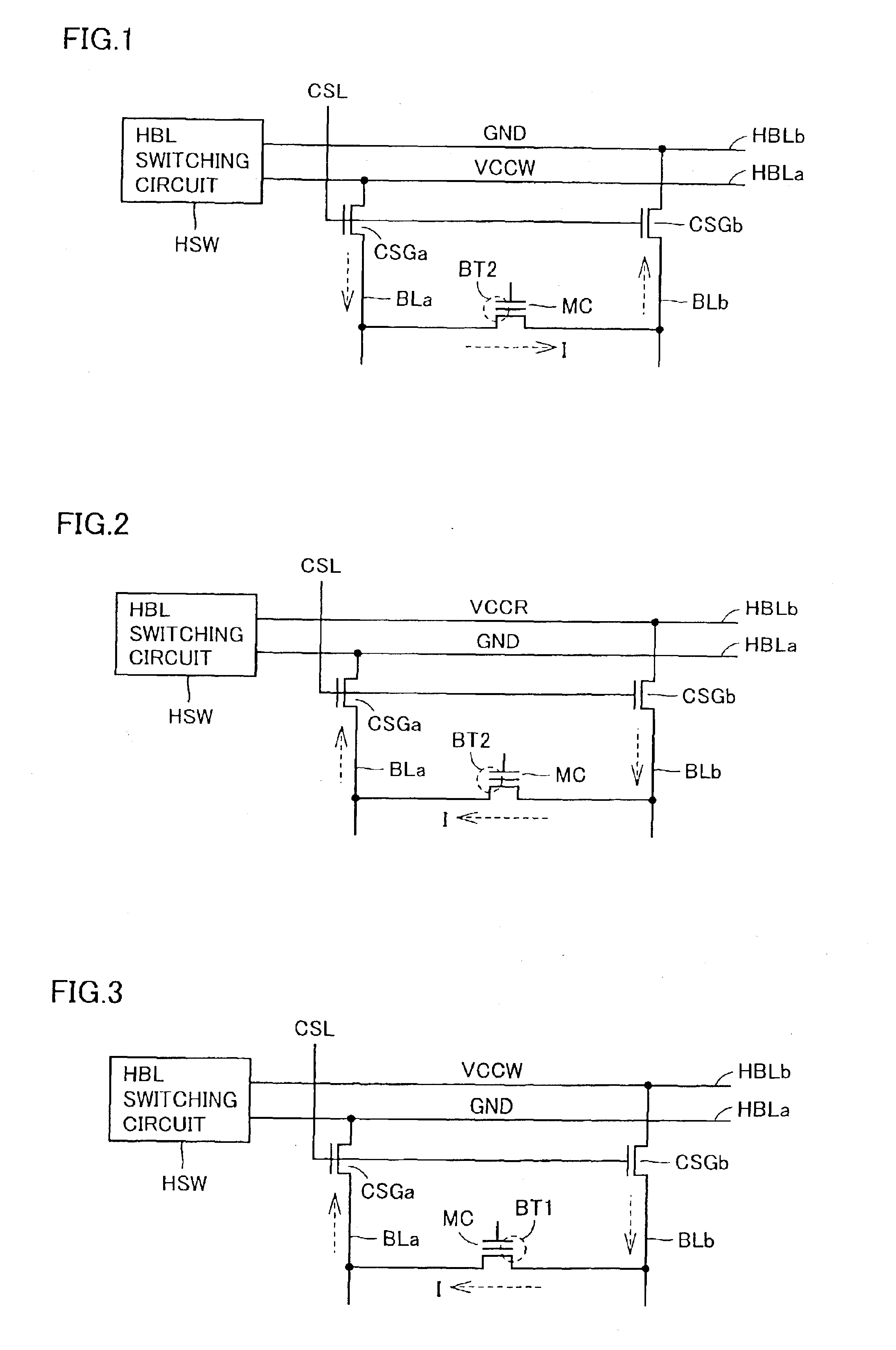
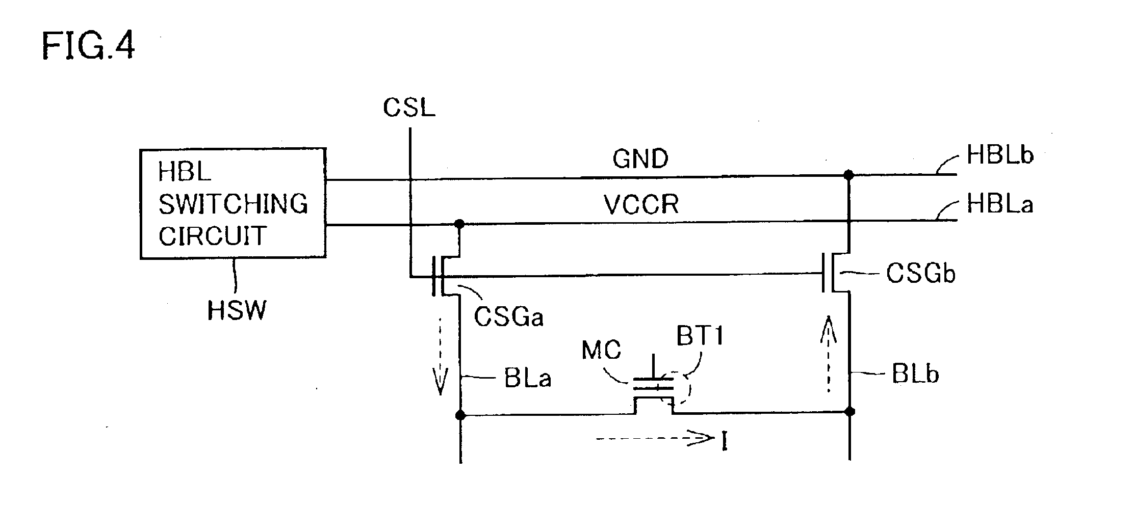
[0073]FIG. 1 is a schematic diagram showing a fundamental configuration of a main part of a nonvolatile semiconductor memory device according to the present invention. In FIG. 1, potential supply lines HBLa and HBLb are commonly disposed to bit lines arranged in one memory block. Voltage levels of potential supply lines HBLa and HBLb are set by HBL switching circuit HSW. HBL switching circuit HSW sets the voltage levels on potential supply lines HBLa and HBLb in accordance with an address signal, a write / read instruction signal, a reverse / forward direction instruction signal and write data.

[0074]While the number of potential supply lines HBL is arbitrary, in order to simplify the description, it is assumed that two potential supply lines are included in potential supply bus HB. Potential supply bus HB is provided for each memory block. Detailed description will be given of arrangement of potential supply buses HB.

[0075]In a memory block provided in correspondence to potential supply...

second embodiment

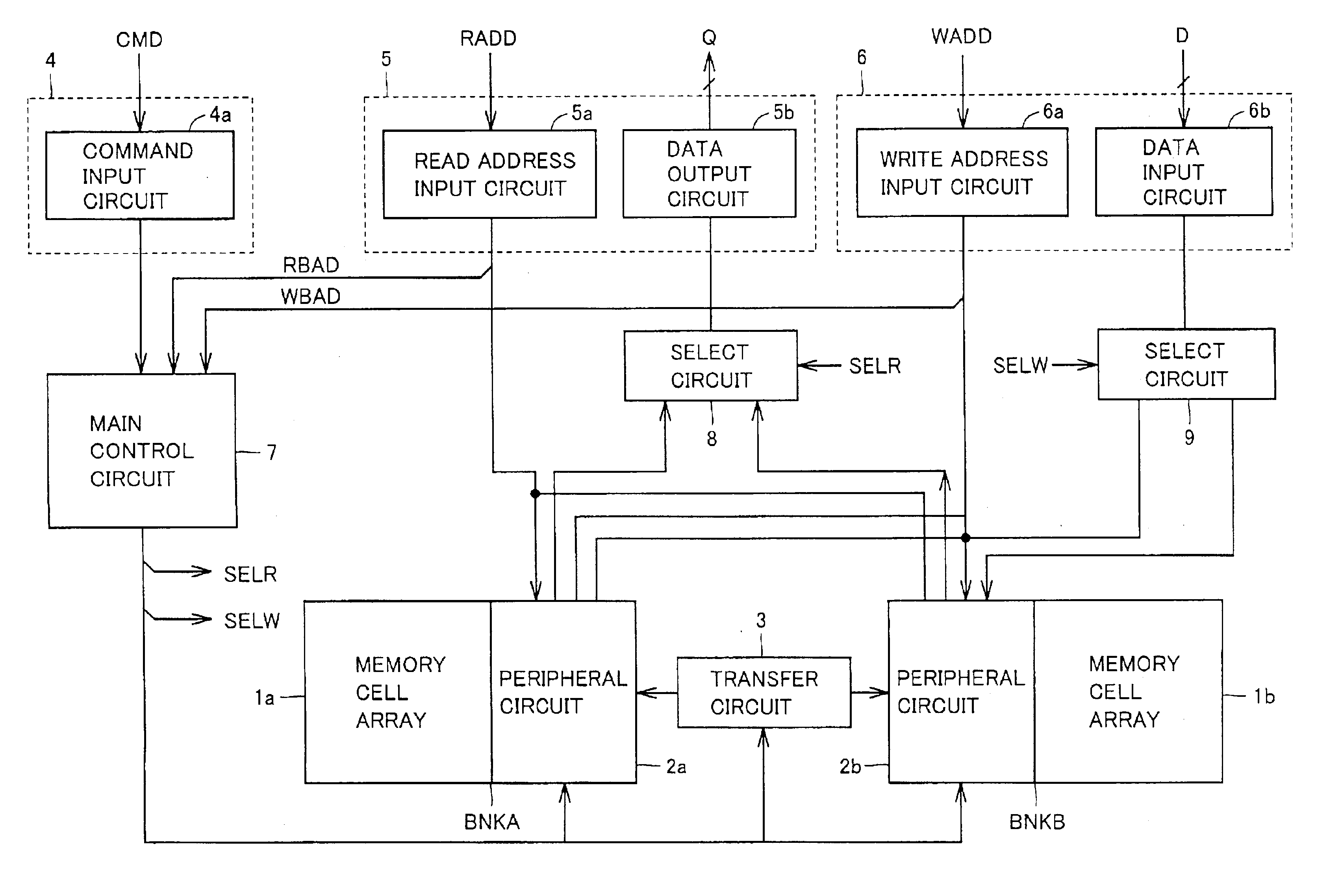
[0258]FIG. 23 is a schematic diagram showing a configuration of a data and address input section of a nonvolatile semiconductor memory device according to a second embodiment of the present invention. In a configuration shown in FIG. 23, there are provided an address / data input port in common to a read port 5 and a write port 6. Specifically, address signal ADD is applied to an address input port 100 and data DQ is supplied to a data input port 102.

[0259]Read port 5 includes: a read address input circuit 5a for taking in an address from address input port 100 in a data read mode, to generate internal read address signal RADD; and a data output circuit 5b for outputting data from select circuit 8 shown in FIG. 6 to data input port 102.

[0260]Write port 6 includes: an address latch 104 for taking in and latching an address from address input port 100, to generate internal write address signal WADD when a hold instruction signal WHLD is active; and a data latch 106 for taking in and lat...


PUM


Abstract

Local buses for performing writing / reading of data are provided in correspondence to memory blocks each having a plurality of nonvolatile memory cells, and also circuits for performing writing / reading of data are provided in correspondence to the memory blocks. In addition, data transfer lines for bidirectionally transferring data are provided commonly to the memory blocks, and transfer switch gates for performing data transfer between the memory blocks are provided commonly to the memory blocks. The memory blocks are divided into banks, writing / reading of data on individual memory blocks are performed in units of banks, and parallel execution of writing and reading or of writing / reading and internal transfer is performed. Thus, it is possible to improve data transfer processing efficiency in a nonvolatile semiconductor device.

Description

BACKGROUND OF THE INVENTION[0001]1. Field of the Invention[0002]The present invention relates to a semiconductor memory device, and particularly to a nonvolatile semiconductor memory device storing data in a nonvolatile manner. More particularly, the present invention relates to a configuration for a data access in a nonvolatile semiconductor memory device with a virtual ground array in which memory cells on adjacent two columns in a row direction are connected to a common bit line.[0003]2. Description of the Background Art[0004]In a nonvolatile semiconductor memory device storing data in a nonvolatile manner, there is known an insulating film charge trap type memory in which charges are trapped in an insulating film under a control gate to store data.[0005]FIG. 25 is a schematic diagram showing a sectional structure of a conventional insulating film charge trap type memory cell. In FIG. 25, an insulating film charge trap type memory cell includes: buried diffusion layers 901a and 9...

Claims


Application Information

Patent Timeline
Patent Type & Authority Patents(United States)
IPC IPC(8): G11C16/10G11C16/06G11C16/02
CPCG11C16/10G11C2216/22
Inventor OOISHI, TSUKASA
Owner RENESAS ELECTRONICS CORP
Why Eureka
Try Eureka