Organo luminescent semiconductor nanocrystal probes for biological applications and process for making and using such probes

a luminescent semiconductor and nanocrystal technology, applied in the field of organic luminescent semiconductor nanocrystal probes, can solve the problems of difficult simultaneous or even non-simultaneous detection or discrimination between the presence of a number, and the limitation of the number of different color organic dye molecules which may be utilized simultaneously or sequentially,

Inactive Publication Date: 2005-08-09
RGT UNIV OF CALIFORNIA
View PDF19 Cites 162 Cited by
  • Summary
  • Abstract
  • Description
  • Claims
  • Application Information

AI Technical Summary

Problems solved by technology

There are a number of problems with such an analytical system.
As a result, there is a severe limitation on the number of different color organic dye molecules which may be utilized simultaneously or sequentially in an analysis since it is difficult to either simultaneously or even non-simultaneously detect or discriminate between the presence of a number of different detectable substances due to the broad spectrum emissions and emission tails of the labelling molecules.
Another problem is that most dye molecules have a relatively narrow absorption spectrum, thus requiring either multiple excitation beams used either in tandem or sequentially for multiple wavelength probes, or else a broad spectrum excitation source which is sequentially used with different filters for sequential excitation of a series of probes respectively excited at different wavelengths.
Another problem frequently encountered with existing dye molecule labels is that of photostability.
In addition, the probe tools used for the study of these systems by electron microscopy techniques are completely different from the probes used for study by fluorescence.
Thus, it is not possible to label a material with a single type of probe for both electron microscopy and for fluorescence.

Method used


Image

  • Organo luminescent semiconductor nanocrystal probes for biological applications and process for making and using such probes
  • Organo luminescent semiconductor nanocrystal probes for biological applications and process for making and using such probes
  • Organo luminescent semiconductor nanocrystal probes for biological applications and process for making and using such probes

Examples


example 1

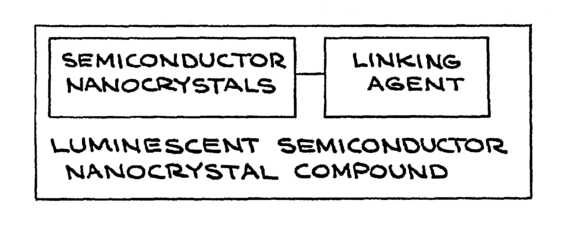
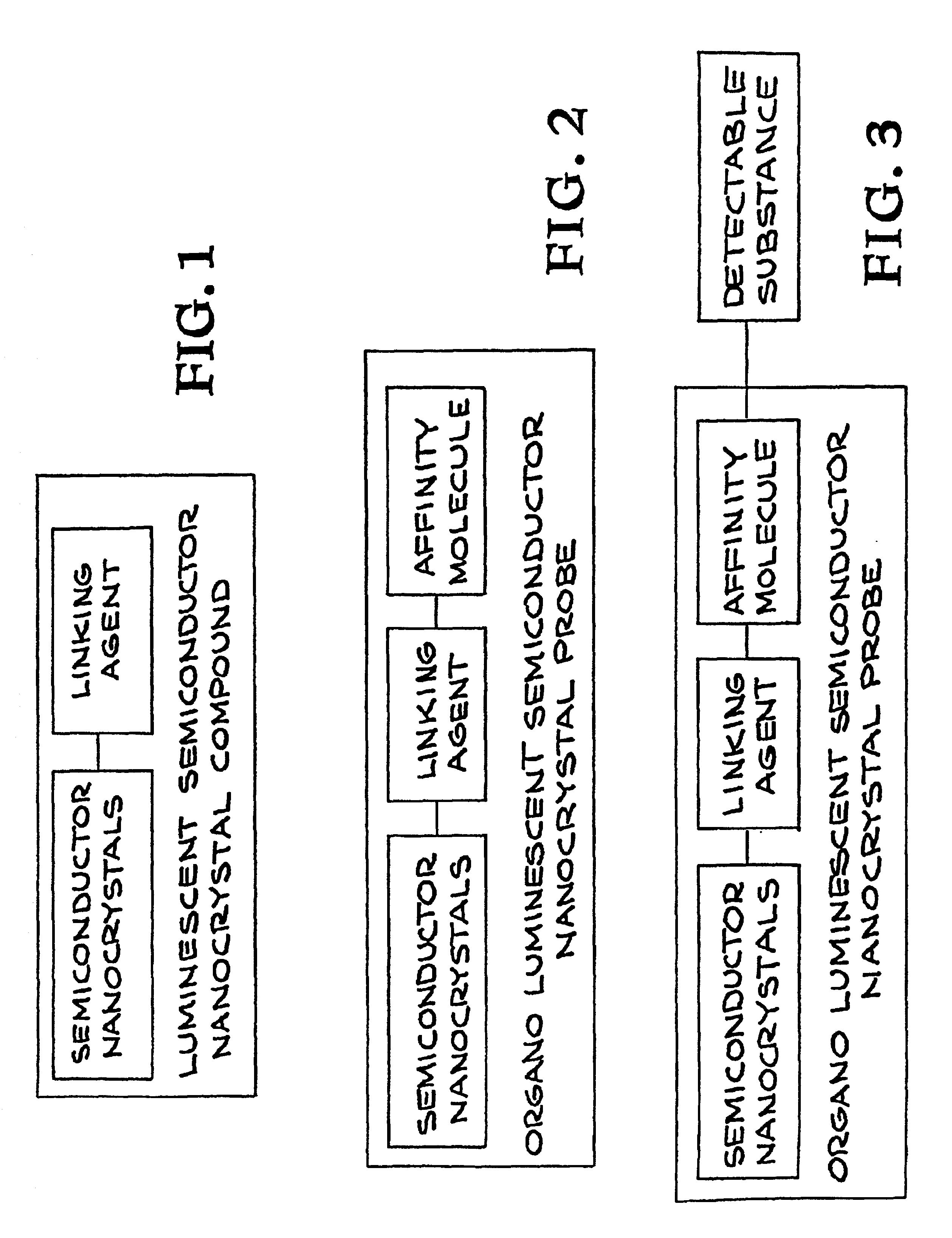
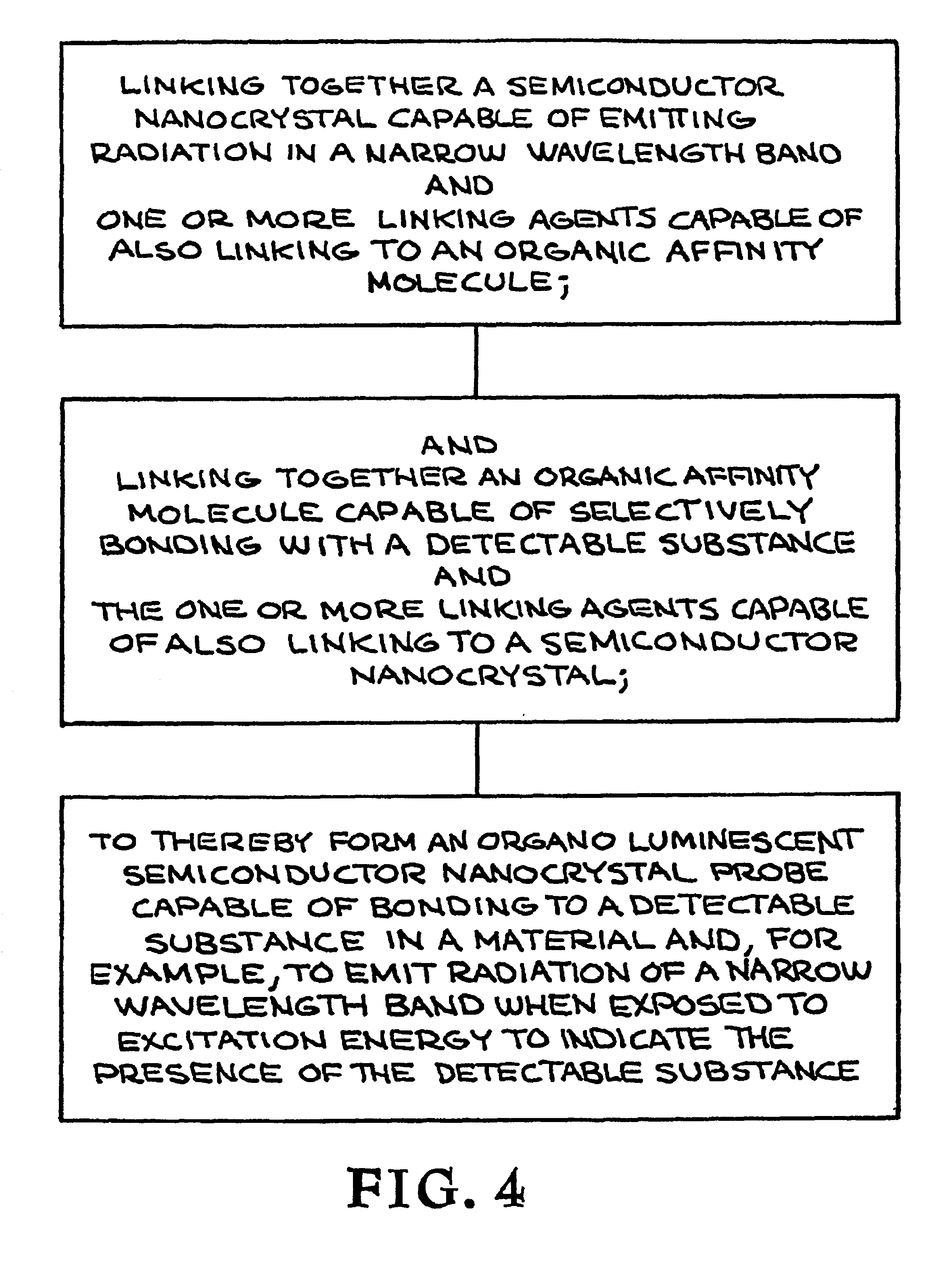
[0052]To illustrate the formation of the luminescent semiconductor nanocrystal compound (comprising the semiconductor nanocrystals linked to a linking agent) 20 ml. of a 5 mM solution of (4-mercapto)benzoic acid was prepared with a pH of 10 using (CH3)4NOH0.5H2O. 20 mg of tris-octylphosphine oxide coated CdSe / CdS core / shell nanocrystals were added to the solution and stirred until completely dissolved. The resultant nanocrystal / linking agent solution was heated for 5 hours at 50-60° C. and then concentrated to a few ml by evaporation. Then an equal volume of acetone was added and the nanocrystals precipitate out of solution homogeneously. The precipitate was then washed with acetone, dried, and then can be stored.

[0053]The luminescent semiconductor nanocrystal compound prepared above can be linked with an appropriate affinity molecule to form the organo luminescent semiconductor nanocrystal probe of the invention to treat a biological material to determine the presence or absence of...

example 2

[0054]To illustrate the formation of luminescent semiconductor nanocrystal compound (comprising glass-coated semiconductor nanocrystals linked to a linking agent), 50 μl of 3-mercaptopropyl-trimethoxy silane was added to 40 ml of an anhydrous solution of 25 vol. % dimethylsulfoxide in methanol, and the pH was adjusted to 10-11 using (CH3)4NOH0.5H2O. 10 mg of tris-octylphosphine oxide coated CdSe / CdS core-shell particles, prepared by the technique described in the aforementioned Peng, Schlamp, Kadavanich, and Alivisatos article, were then dissolved in this solution, and stirred for several hours. The solution was diluted with 40 ml of methanol adjusted to a pH of 10 with (CH3)4NOH0.5H2O, and heated for 1 hour at 69° C. The solution was stirred for an hour, and 40 ml of a 90 vol. % methanol / 9.89 vol. % H2O / 0.1 vol. % trimethoxysilylpropyl urea / 0.01 vol. % aminopropyl-trimethoxy silane solution which had been stirring for at least an hour, was added, and stirred for 2 hours. Subsequent...


PUM

PropertyMeasurementUnit
thicknessaaaaaaaaaa
thicknessaaaaaaaaaa
sizeaaaaaaaaaa

Abstract

A semiconductor nanocrystal compound is described capable of linking to an affinity molecule. The compound comprises (1) a semiconductor nanocrystal capable of emitting electromagnetic radiation and / or absorbing energy, and / or scattering or diffracting electromagnetic radiation—when excited by an electromagnetic radiation source or a particle beam; and (2) at least one linking agent, having a first portion linked to the semiconductor nanocrystal and a second portion capable of linking to an affinity molecule. The compound is linked to an affinity molecule to form a semiconductor nanocrystal probe capable of bonding with a detectable substance. Subsequent exposure to excitation energy will excite the semiconductor nanocrystal in the probe causing the emission of electromagnetic radiation. Further described are processes for respectively: making the luminescent semiconductor nanocrystal compound; making the semiconductor nanocrystal probe; and using the probe to determine the presence of a detectable substance in a material.

Description

CROSS-REFERENCE TO RELATED APPLICATION[0001]This application is a continuation of U.S. patent application Ser. No. 09 / 349,833 filed Jul. 8, 1999 now U.S. Pat. No. 6,423,551 which application is a continuation of U.S. patent application Ser. No. 08 / 978,450 filed Nov. 25, 1997, and now issued as U.S. Pat. No. 5,990,479 on Nov. 23, 1999.[0002]The invention described herein arose in the course of, or under, Contract No. DE-AC03-SF00098 between the United States Department of Energy and the University of California for the operation of the Ernest Orlando Lawrence Berkeley National Laboratory. The Government may have rights to the invention.BACKGROUND OF THE INVENTION[0003]1. Field of the Invention[0004]This invention relates to organo luminescent semiconductor nanocrystal probes for biological applications wherein the probes includes a plurality of semiconductor nanocrystals capable of luminescence and / or absorption and / or scattering or diffraction when excited by a radiation or particle...

Claims


Application Information

Patent Timeline
Patent Type & Authority Patents(United States)
IPC IPC(8): G01N33/543G01N33/58C12Q1/68G01N33/533G01N33/542G01Q70/08G01Q70/18
CPCB82Y15/00G01N33/533G01N33/542G01N33/54373G01N33/588C12Q1/6816Y10T436/24Y10T428/2993Y10T428/2991Y10T428/2996Y10T428/2989Y10T428/2982Y10T428/2995C12Q2563/107
Inventor WEISS, SHIMONBRUCHEZ, JR., MARCELALIVISATOS, PAUL
Owner RGT UNIV OF CALIFORNIA
Why Eureka
Try Eureka