Electron beam apparatus and spacer for reducing electrostatic charge

a technology of electrostatic charge and electron beam, which is applied in the field of electron beam apparatus and image producer to achieve the effect of reducing the surface

Inactive Publication Date: 2005-08-09
CANON KK
View PDF19 Cites 37 Cited by
  • Summary
  • Abstract
  • Description
  • Claims
  • Application Information

AI Technical Summary

Benefits of technology

[0070]Those are the methods for relaxing the uniformity of incident angle itself and for reducing surface effect as a property on material side, that is, the ratio of penetration depth of primary electrons to penetration depth of secondary electrons: d / λ.(1) Dispersion of Incident Angle of Primary Electrons
[0071]Incident angle is allowed to have an infinitesimal distribution in the normal direction on the interface considered as a surface, so that it is not restricted to the angle specified by the outside. Thus the incident angle defined on a local basis has a distribution with respect to the angle defined on a broader basis, which allows dependency on incident angle to be relaxed. Since dependency on incident angle shows the property of rapidly increasing when incident angle is close to 90 degrees, relaxation by the dispersion of incident angle is significantly effective.(2) Reduction of the Ratio of Penetration Depth of Primary Electrons to Penetration Depth of Secondary Electrons
[0082]Both of the primary and secondary electrons traveling in the highly resistive film portion gradually lose their energy while interacting with the atoms within the medium and repeating collision and scattering. In such a situation, their penetration depth and energy decreasing rate largely depend on the electron density of the medium they pass through. In the medium having a high electron density, since the probability of their scattering is high, their penetration depth becomes small. In addition, since the energy decreasing rate for a certain penetration distance is large, the amount of secondary electrons generated for unit depth increases. Thus, in the structure having a high electron density, in other words, in the material having a large specific gravity, penetration depth of electrons is smaller and the amount of secondary electrons generated within the medium is larger than those in the material having a small specific gravity.
[0113]In each of the above inventions, multiple rows of emission elements and multiple columns of electron emission devices are wired in a matrix can be suitably employed as an electron source. The electron source can be constructed in a simple matrix.

Problems solved by technology

This is a significant cause of positive electrification of spacers within image displays of the electron beam emission type where many electrons enter the surface of the spacer at an angle.

Method used


Image

  • Electron beam apparatus and spacer for reducing electrostatic charge
  • Electron beam apparatus and spacer for reducing electrostatic charge
  • Electron beam apparatus and spacer for reducing electrostatic charge

Examples


example 1

Alumina Substrate, Board-shaped, Ruthenium Oxide Paste

[0306]The spacer used in this example was produced as described below.

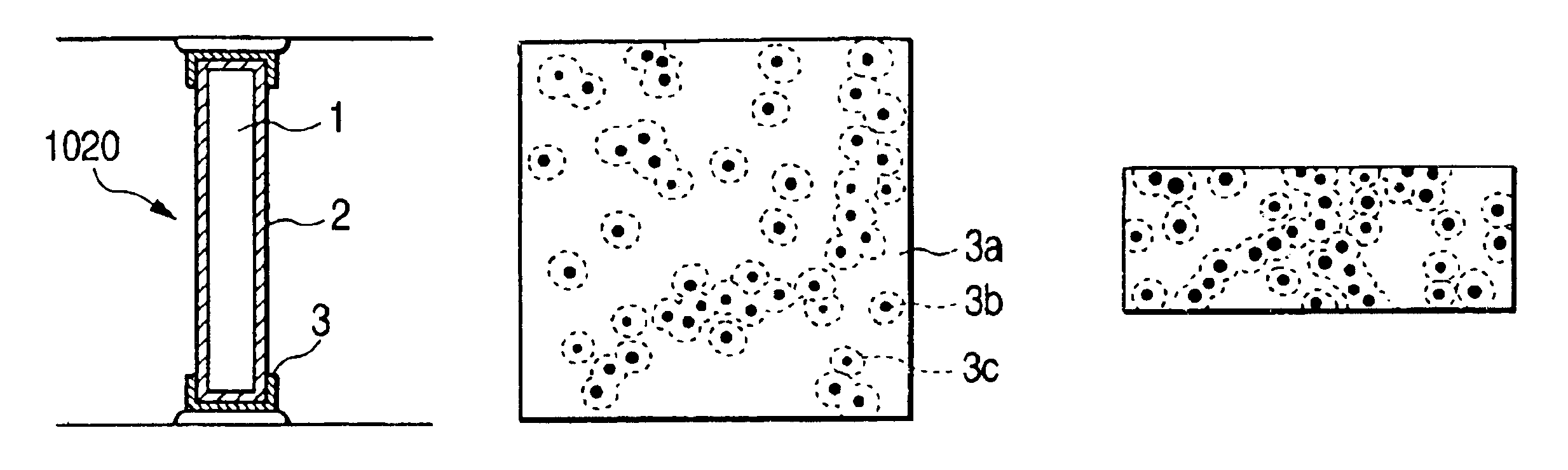
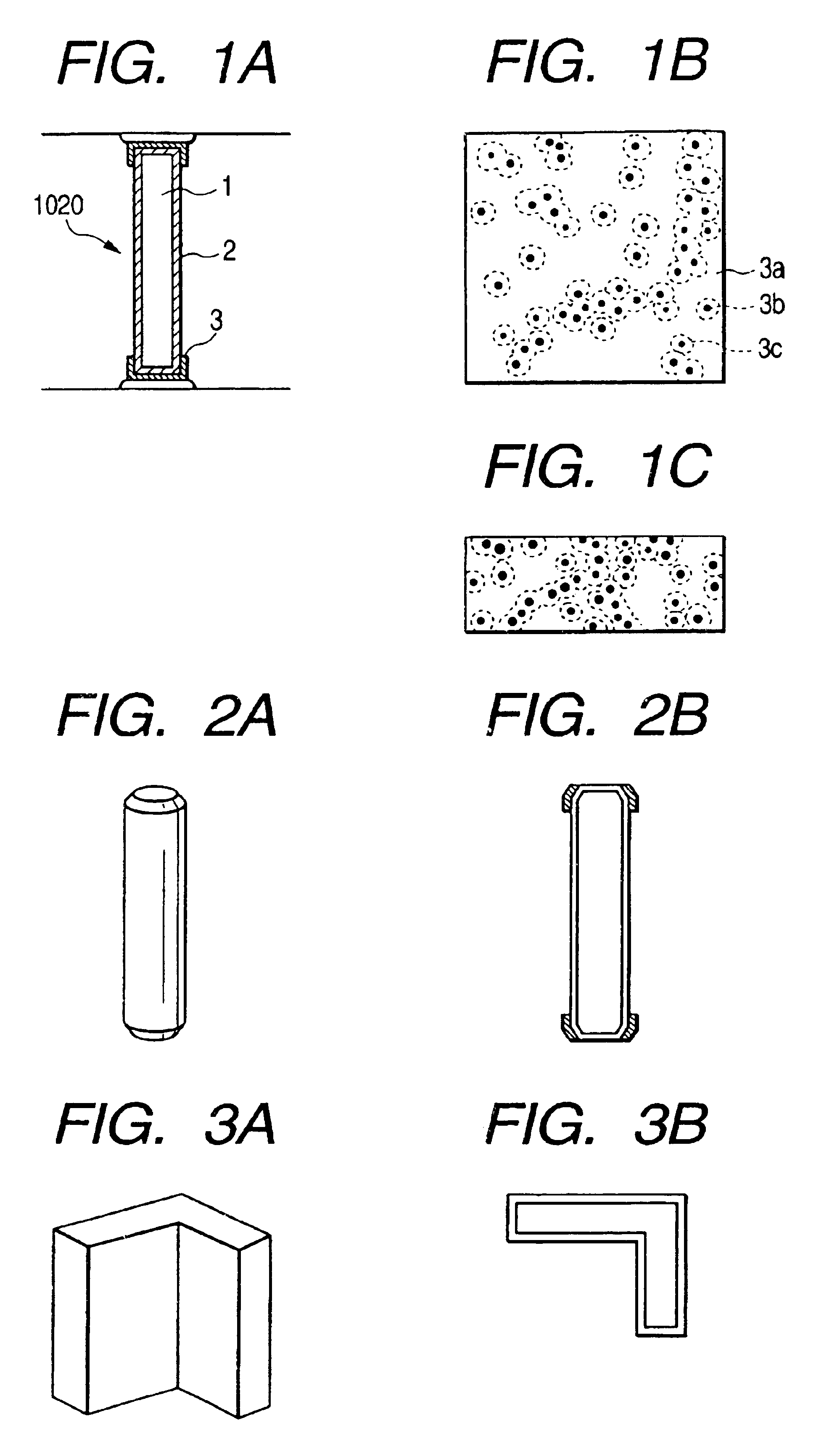
[0307]As an original, used was a ceramic substrate produced with ratio of zirconia and alumina as 65:35, to have the same thermal expansion coefficient as a soda-lime glass substrate which was the same material of the rear plate. The original was subjected to polishing so that its outside dimensions of thickness, height and length would be 0.2 mm, 3 mm, and 40 mm, respectively. The average roughness of the substrate surface thus formed was 300 Å. Hereinafter the substrate is referred to as a0.

[0308]Prior to deposition processing, the above spacer substrate a0 was subjected to first ultrasonic cleaning in deionized water, IPA and acetone for 3 minutes, then drying at 80° C. for 30 minutes, and followed by UV ozone cleaning so as to remove organic residues on the surface of the substrate.

[0309]Then the surface was coated with 1108 resistive paste from DuPont by p...

example 2

Low-alkali Substrate, Board-shaped, Ruthenium Oxide

[0324]As an original, used was a low-alkali glass substrate, which was subjected to injection molding and mirror surface polishing so that its outside dimensions of thickness, height and length would be 0.2 mm, 3 mm, and 40 mm, respectively. The average roughness of the substrate surface thus formed was 100 Å. Hereinafter the substrate is referred to as g0. Prior to deposition processing, the above spacer substrate g0 was subjected to first ultrasonic cleaning in deionized water, IPA and acetone for 3 minutes, then drying at 80° C. for 30 minutes, and followed by UV ozone cleaning so as to remove organic residues on the surface of the substrate.

[0325]Then the surface was coated with a highly resistive film and a low resistive film was partly formed thereon in the same manner as Example 1, except that the above glass substrate g0 was used as a spacer substrate and that the upper limit of heating temperature was set for 600° C. almost...


PUM


Abstract

An electron beam apparatus including a hermetic container provided with an electron source, in which, when a first member is arranged in the hermetic container, at least part of the first member is coated with a film, and the film is configured in such a manner that it includes two regions, a first region and a second region different in electron density from the first region and the second region forms a network in the first region. This three-dimensional network structure allows a member being charged to be preferably controlled. Thereby, it is possible to control the effects of a member being charged which is used in an electron beam apparatus.

Description

BACKGROUND OF THE INVENTION[0001]1. Field of the Invention[0002]The present invention relates to an electron beam apparatus and an image producer as an application thereof, such as an image display and the like. The present invention also relates to a spacer for use in the electron beam apparatus.[0003]2. Related Background Art[0004]There are two types of electron emission devices currently known: a hot cathode element and a cold cathode element. As to the latter, the known elements include, for example, surface conduction type electron emission devices, field emission elements (hereinafter referred to as an FE type) and metal-insulating layer-metal type electron emission devices (hereinafter referred to as an MIM type).[0005]The surface conduction type electron emission devices currently known include, for example, one disclosed by M. I. Elinson in Radio Eng. Electron Phys., 10, 1290, (1965), and the others described below.[0006]The surface conduction type electron emission devices...

Claims


Application Information

Patent Timeline
Patent Type & Authority Patents(United States)
IPC IPC(8): H01J29/02H01J9/24H01J5/03H01J29/86H01J29/87H01J31/12
CPCH01J29/028H01J29/864H01J31/127H01J2329/863H01J2329/864H01J2329/8645H01J2329/8655H01J2329/866
Inventor ITO, NOBUHIROMITSUTAKE, HIDEAKI
Owner CANON KK
Why Eureka
Try Eureka