
Thin-film magnetic head and method of manufacturing same, head gimbal assembly, and hard disk drive

a technology of thin film and magnetic head, which is applied in the direction of maintaining head carrier alignment, nanoinformatics, instruments, etc., can solve the problems of increasing the signal-to-noise ratio, and increasing the thickness so as to reduce the resistance of the conductive layer and satisfy the magnetic signal reading characteristics.

Inactive Publication Date: 2005-08-09
TDK CORPARATION
View PDF8 Cites 5 Cited by
  • Summary
  • Abstract
  • Description
  • Claims
  • Application Information

AI Technical Summary

Benefits of technology

[0022]It is an object of the invention to provide a thin-film magnetic head and a method of manufacturing same, a head gimbal assembly and a hard disk drive, for achieving satisfactory magnetic signal reading characteristics by preventing conductive layers, which are used for feeding a current for magnetic signal detection to a magnetoresistive element, from being damaged during processing of a medium facing surface, while sufficiently lowering the resistance of the conductive layers.
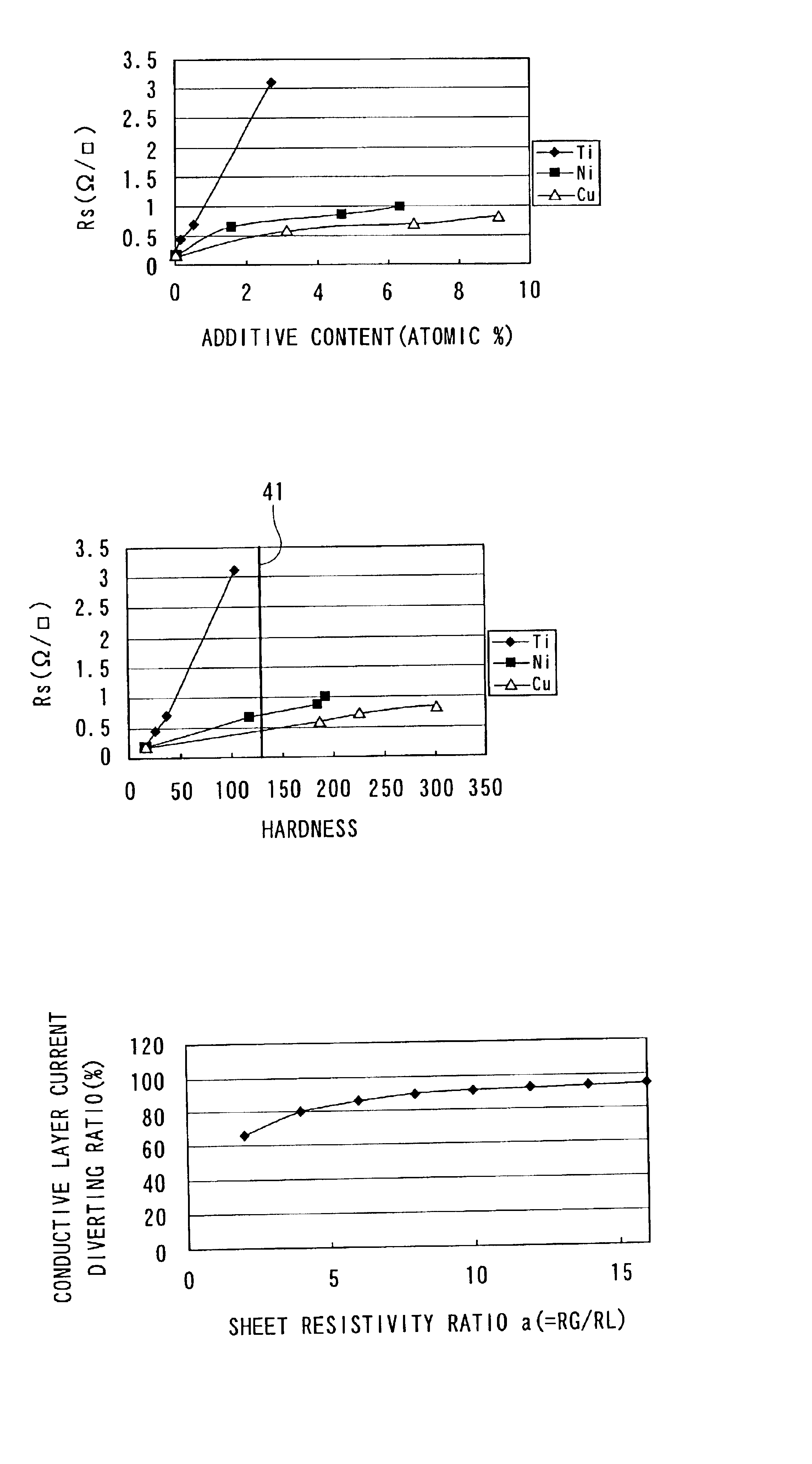
[0026]According to the first thin-film magnetic head or the first method, the conductive layers are each made of a gold alloy having a resistivity of less than 22 μΩ·cm and a hardness as high as or higher than a hardness of a material used for making the bias field applying layers. Hence, the resistivity of each of the conductive layers is smaller than the resistivity of a conductive layer made of a laminate of a TiW layer and a Ta layer. In addition, the hardness of the conductive layers is as high as or higher than the hardness of the bias field applying layers, which prevents the conductive layers from being damaged during processing of the medium facing surface.
[0031]According to the second thin-film magnetic head or the second method, the conductive layers are each made of a gold alloy having a resistivity of less than 22 μΩ·cm and a hardness higher than that of gold. Hence, the resistivity of each of the conductive layers is smaller than the resistivity of a conductive layer made of a laminate of a TiW layer and a Ta layer. In addition, the hardness of the conductive layers is higher than the hardness of a conductive layer made of gold, which prevents the conductive layers from being damaged during processing of the medium facing surface.
[0034]According to the head gimbal assembly or the hard disk drive of the invention, the conductive layers are each made of a gold alloy having a resistivity of less than 22 μΩ·cm and a hardness as high as or higher than a hardness of a material used for making the bias field applying layers. Hence, the resistivity of each of the conductive layers is smaller than the resistivity of a conductive layer made of a laminate of a TiW layer and a Ta layer. In addition, the hardness of the conductive layers is as high as or higher than the hardness of the bias field applying layers, which prevents the conductive layers from being damaged during processing of the medium facing surface.

Problems solved by technology

If Barkhausen noise occurs, an abrupt variation in output results, which induces a reduction in signal-to-noise ratio (hereinafter called S / N ratio) and an increase in error rate.
However, increasing the thickness of the conductive layers has a process limitation.
A first problem is that, during lapping of the medium facing surface, the conductive layers extend in the medium facing surface and adhere to the MR element.
This causes a resistance value of the MR element to change, which results in variations in the characteristics of the read head.
A second problem is that lapping of the medium facing surface causes the conductive layers to be abraded more than the other layers, which results in a difference in level between each of the conductive layers and the other layers in the medium facing surface, with the end of each of the conductive layers recessed from the ends of the other layers in the medium facing surface.
As a result, corrosion may occur at the gap portion and spread toward the MR element.
Conductive layers made of a Cu layer have smaller resistivity compared with the conductive layers made of an Au layer, but they are vulnerable to oxidation and therefore have poorer resistance to corrosion.

Method used


Image

  • Thin-film magnetic head and method of manufacturing same, head gimbal assembly, and hard disk drive
  • Thin-film magnetic head and method of manufacturing same, head gimbal assembly, and hard disk drive
  • Thin-film magnetic head and method of manufacturing same, head gimbal assembly, and hard disk drive

Examples


Embodiment Construction

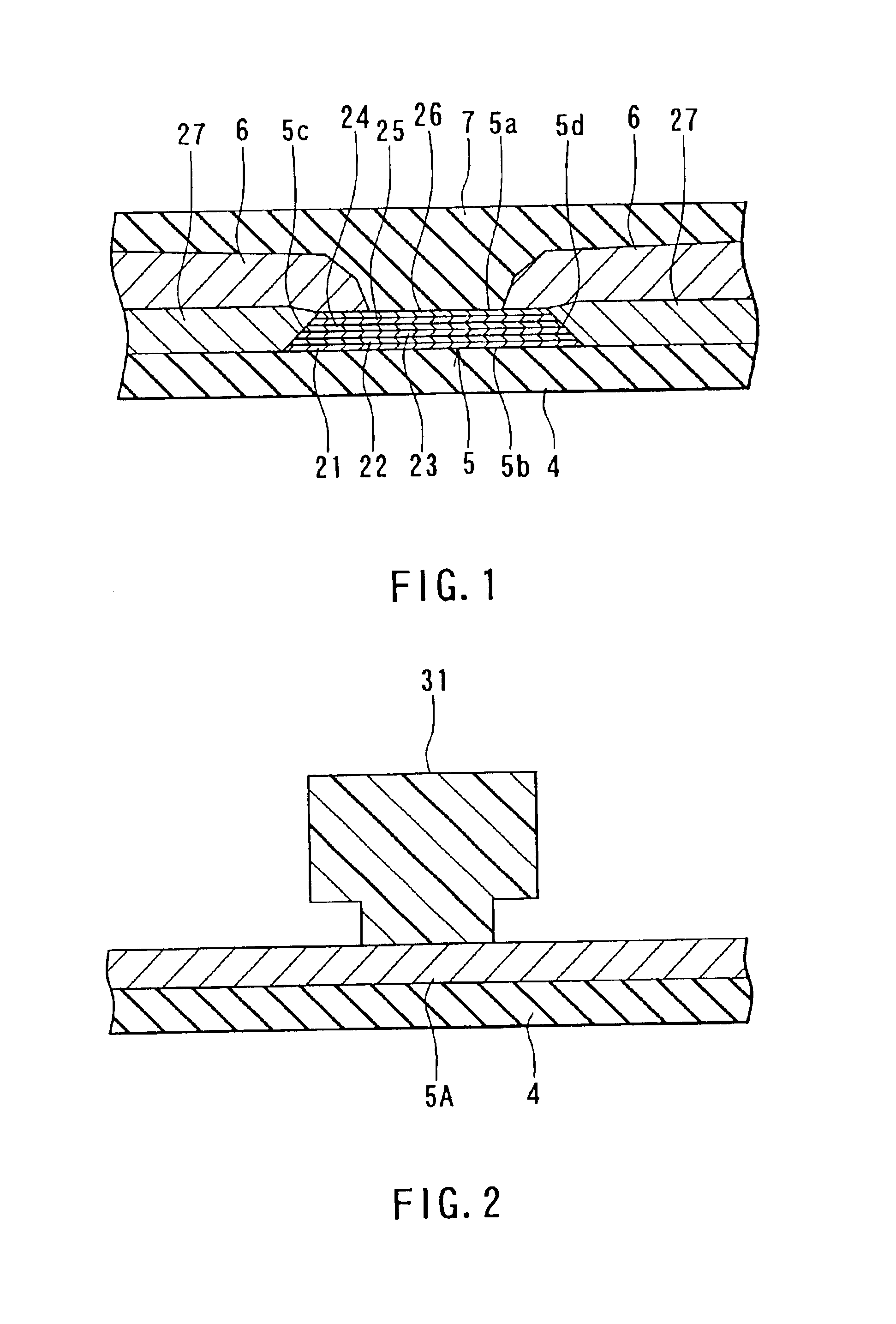
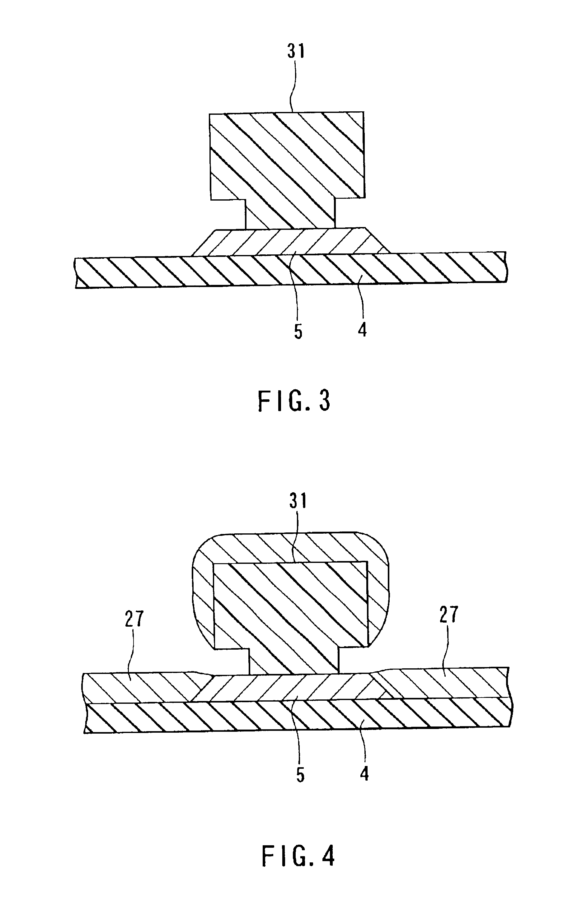
[0056]A preferred embodiment of the invention will now be described in detail with reference to the accompanying drawings. Reference is now made to FIGS. 6A to 11A and FIGS. 6B to 11B to describe a thin-film magnetic head and an outline of a method of manufacturing the same according to the embodiment of the invention. FIGS. 6A to 11A are cross sections each orthogonal to the air bearing surface. FIGS. 6B to 11B are cross sections of the magnetic pole portion each parallel to the air bearing surface.

[0057]In the manufacturing method, as shown in FIGS. 6A and 6B, an insulating layer 2 of an insulating material such as alumina (Al2O3) is formed to a thickness of 1 to 5 μm, for example, by sputtering or the like on a substrate 1 of a ceramic material such as aluminum oxide and titanium carbide (Al2O3—TiC). On the insulating layer 2, a bottom shield layer 3 of a magnetic material such as Permalloy (NiFe) is formed to a thickness of about 3 μm, for example, by sputtering, plating or the ...


PUM


Abstract

A read head comprises an MR element, two bias field applying layers, and two conductive layers. The two bias field applying layers are adjacent to both side portions of the MR element, and apply a bias magnetic field to the MR element along the longitudinal direction. The two conductive layers feed a sense current to the MR element, each of the conductive layers being disposed to be adjacent to one of surfaces of each of the bias field applying layers and to overlap one of surfaces of the MR element. The conductive layers are each made of a gold alloy having a resistivity of less than 22 μΩ·cm and a hardness as high as or higher than the hardness of a material used for making the bias field applying layers.

Description

BACKGROUND OF THE INVENTION[0001]1. Field of the Invention[0002]The present invention relates to a thin-film magnetic head that incorporates a magnetoresistive element for reading a magnetic signal and a method of manufacturing such a thin-film magnetic head, a head gimbal assembly and a hard disk drive incorporating the thin-film magnetic head.[0003]2. Description of the Related Art[0004]Performance improvements in thin-film magnetic heads have been sought as a real recording density of hard disk drives has increased. Such thin-film magnetic heads include composite thin-film magnetic heads that have been widely used. A composite head is made of a layered structure including a read (reproducing) head having a magnetoresistive element (that may be hereinafter called an MR element) for reading and a write (recording) head having an induction-type electromagnetic transducer for writing, the read head and the write head being stacked on a substrate.[0005]MR elements include: an AMR elem...

Claims


Application Information

Patent Timeline
IPC IPC(8): G11B5/596G11B5/39
CPCB82Y10/00B82Y25/00G11B5/3903G11B5/3909G11B5/59683G11B2005/3996
Inventor ITO, NORIYUKITANAKA, KOSUKETERUNUMA, KOICHI
Owner TDK CORPARATION
Learn More