Method for array processing of surface acoustic wave devices
- Summary
- Abstract
- Description
- Claims
- Application Information
AI Technical Summary
Benefits of technology
Problems solved by technology
Method used
Image
Examples
Embodiment Construction
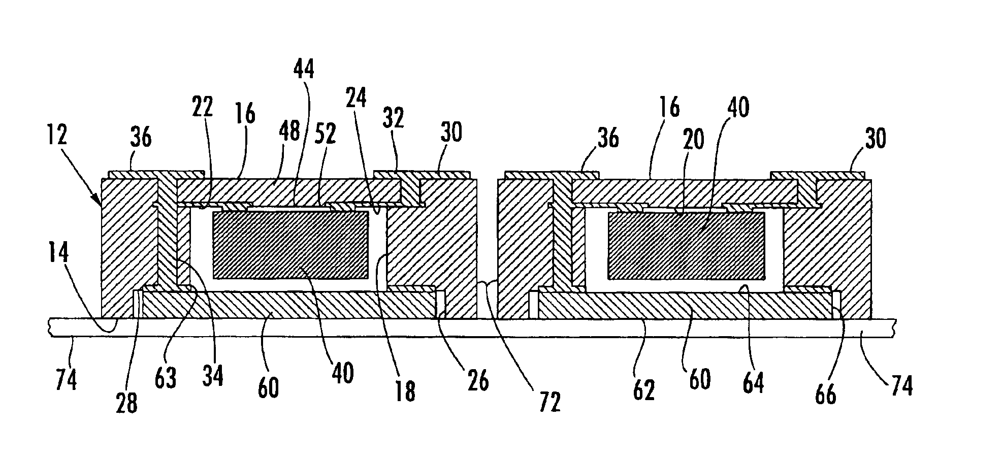
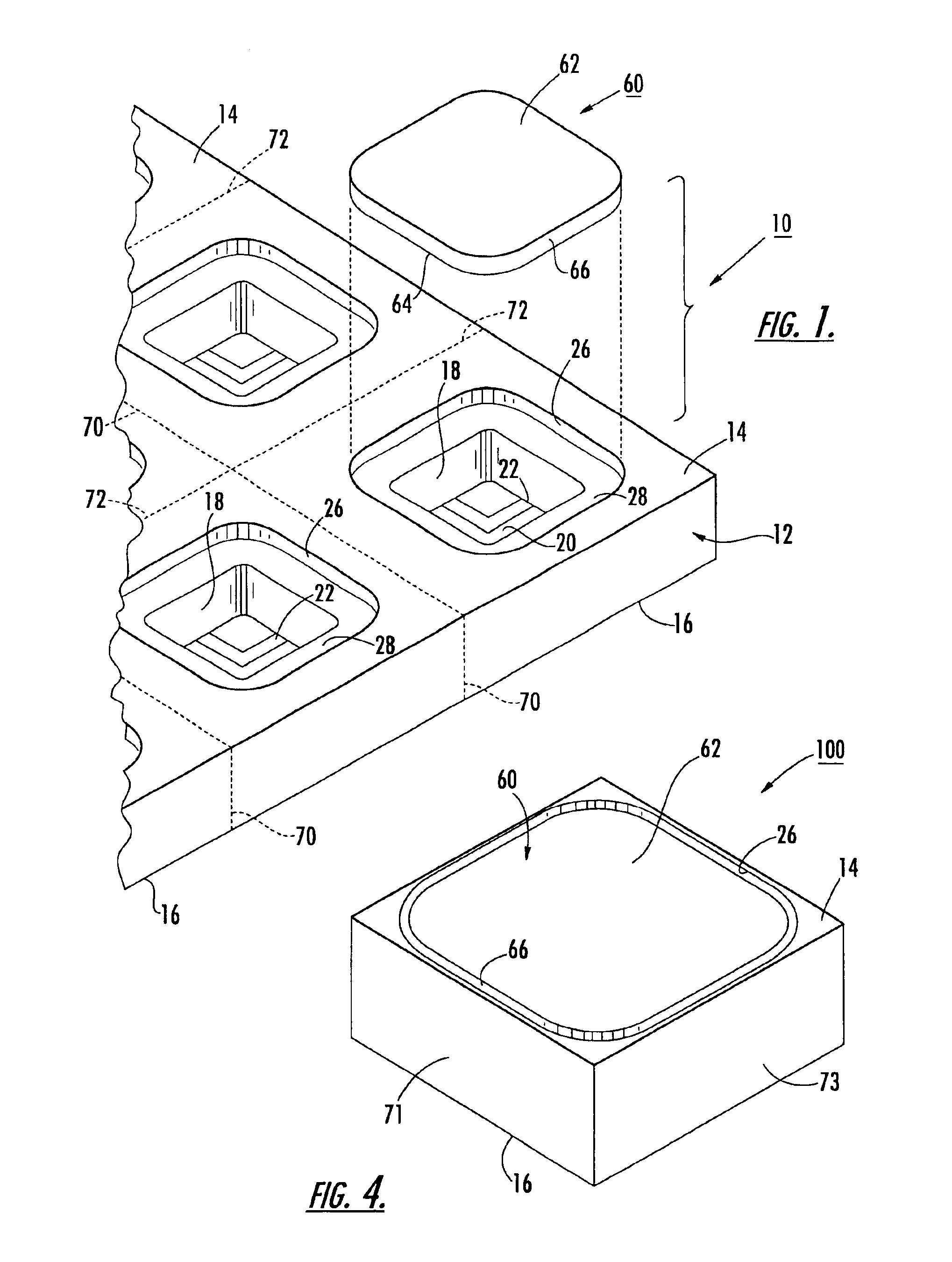
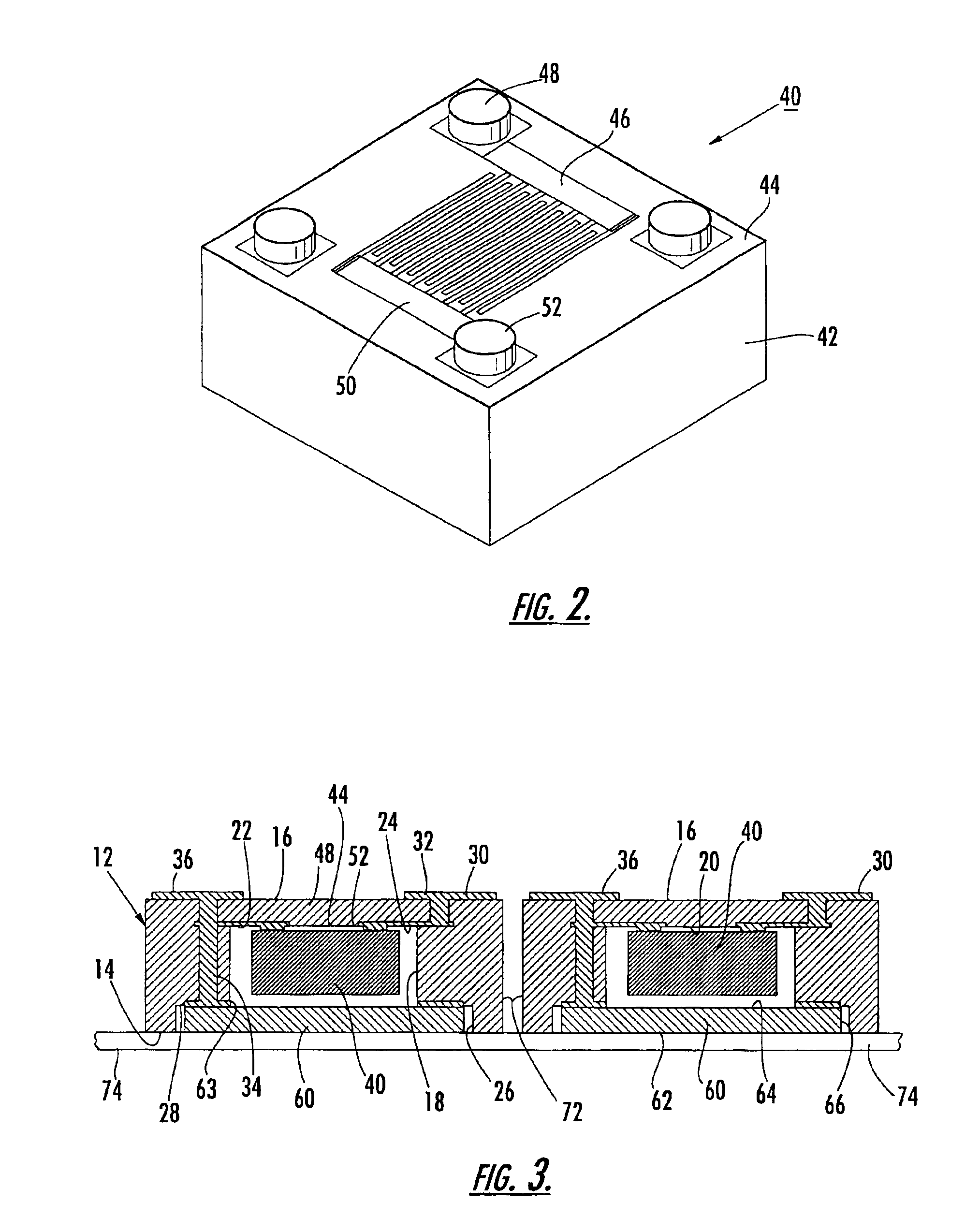
[0021]A system and method for array processing of surface acoustic wave devices in accordance with this invention will now be described with reference to FIGS. 1-4.
[0022]In FIG. 1, the assembly used in practicing the method is referred to generally with reference numeral 10. The assembly 10 includes an array formed in a ceramic body 12 having an upper surface 14 and a lower surface 16. The array includes plural cavities 18, each extending into the ceramic body 12 from the upper surface 14 to a cavity bottom 20. As thus configured, there is a small dimension of the ceramic body 12 between the cavity bottom 20 and the second surface 16 (note the cross-section of FIG. 3).
[0023]The assembly is provided with at least two conductive paths extending from the interior of each cavity 18 to a surface of the ceramic body 12. As shown in FIGS. 1-4, these conductive paths are provided by conductive layers 22, 24 on the bottom 20 of the cavity 18, which are respectively electrically connected to ...
PUM
| Property | Measurement | Unit |
|---|---|---|
| Electrical conductivity | aaaaa | aaaaa |
| Electrical conductor | aaaaa | aaaaa |
| Area | aaaaa | aaaaa |
Abstract
Description
Claims
Application Information


