Methods of forming nitride films

Inactive Publication Date: 2005-08-16
AVIZA TECHNOLOGY INC
View PDF26 Cites 12 Cited by
  • Summary
  • Abstract
  • Description
  • Claims
  • Application Information

AI Technical Summary

Benefits of technology

[0019]From a still further aspect the invention consists in a silicon nitride film having reduced Si—H and N—H bonding, particularly as shown by FTIR bonding peak area analysis. Thus the Si—H:Si—N bonding peak area ratio may be <0.02, whilst the N

Problems solved by technology

In general molecular nitrogen is disregarded as a nitrogen source as the triple bonding of the nitrogen gas makes it unusually stable and difficult to dissociate.
Indeed it i

Method used


Image

  • Methods of forming nitride films
  • Methods of forming nitride films
  • Methods of forming nitride films

Examples


Embodiment Construction

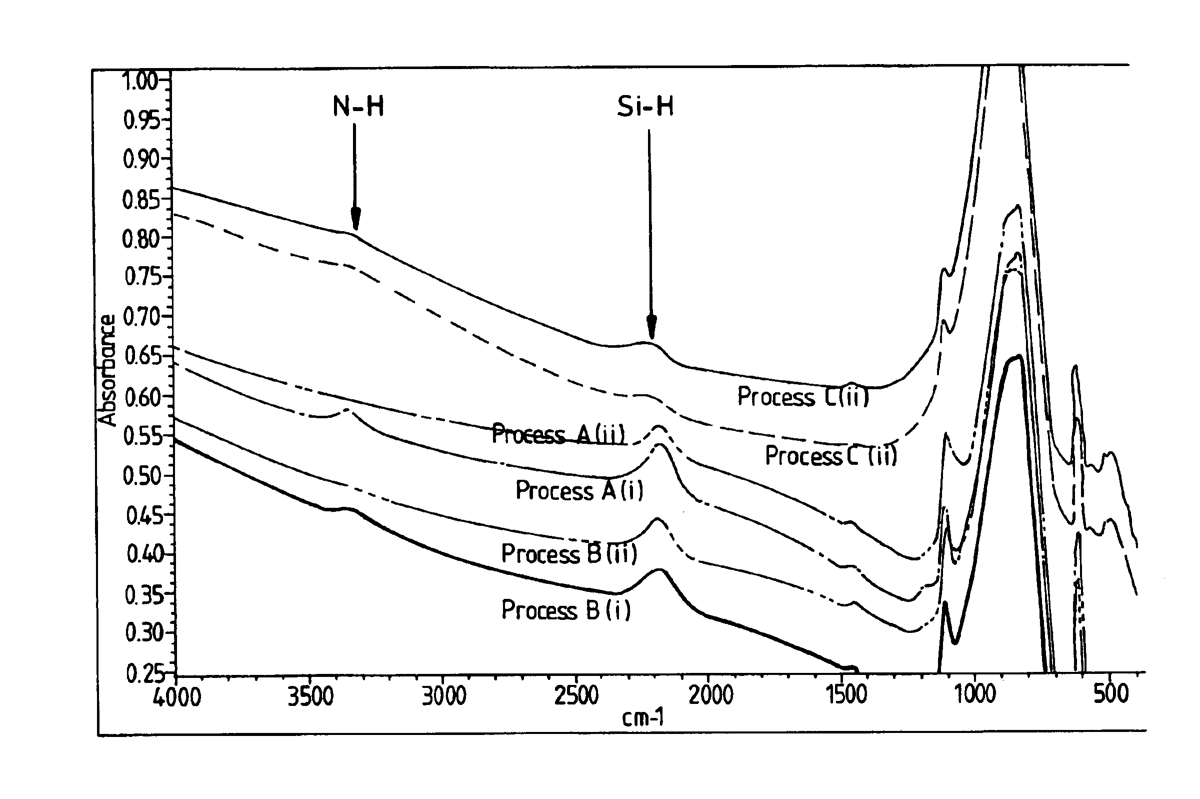
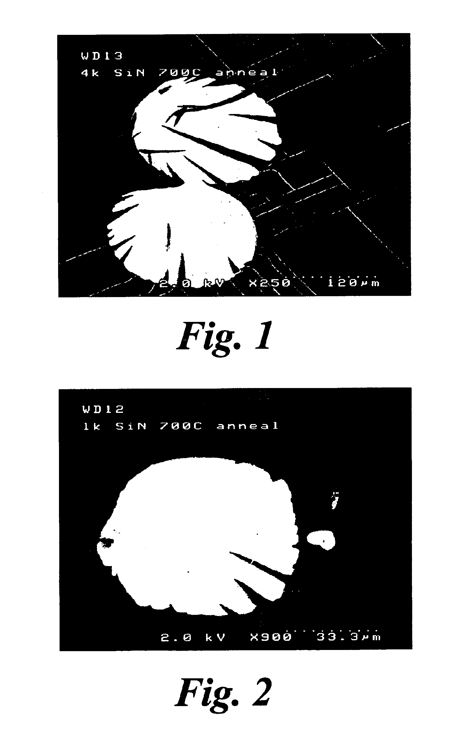
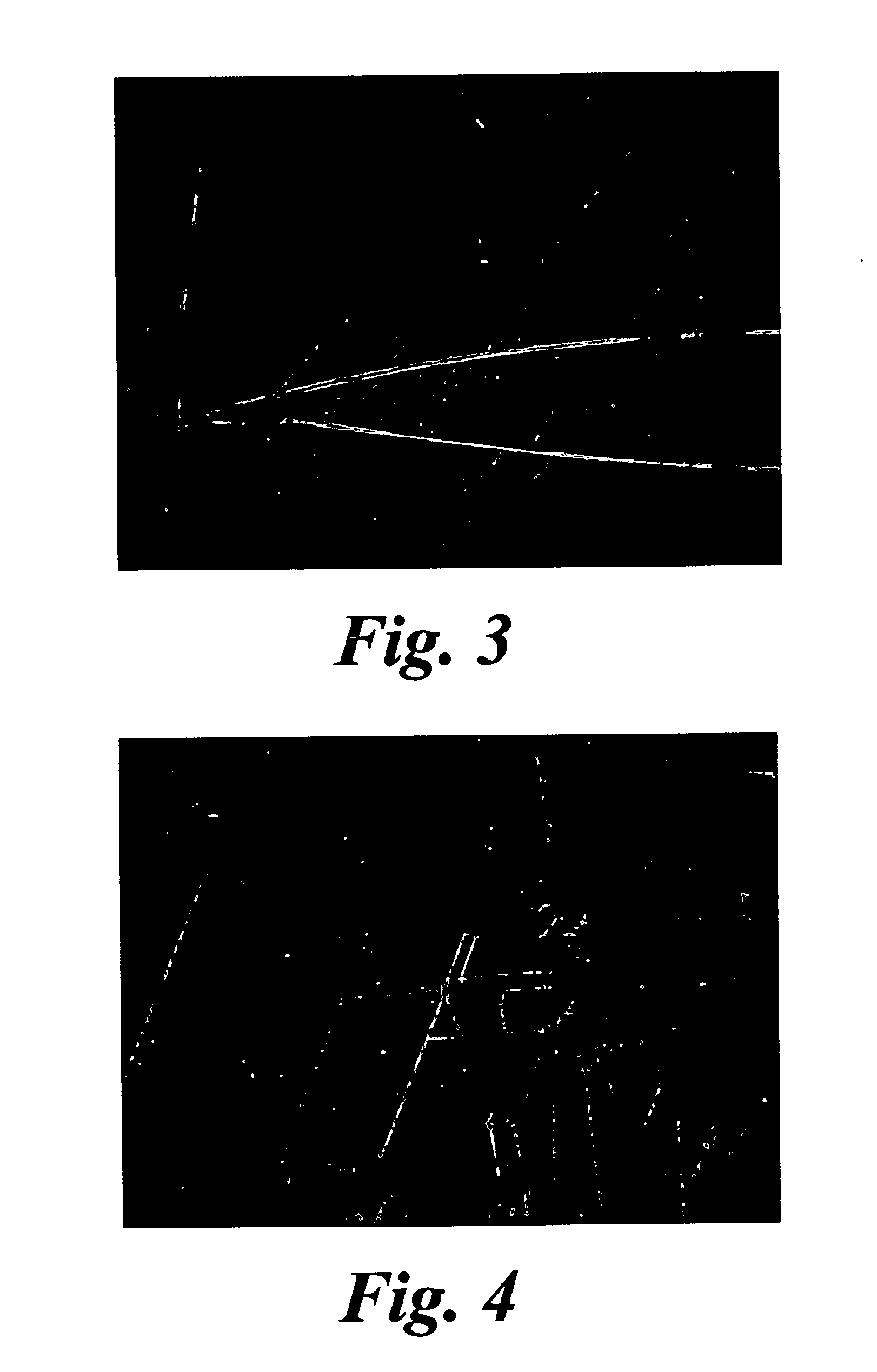
[0027]The applicants wish to deposit stochiometric silicon nitride on gallium arsenide for the reasons already described. The presence of stochiometric silicon nitride is generally indicated by a refractive index of 2. The applicants are seeking, therefore, an acceptable film having such a refractive index and good (e.g. across the wafer) uniformity.

[0028]The applicants began their experiments with a standard silicon nitride capping process as defined in Table 1 below and this resulted in a film having the properties shown in Table 2 below.

[0029]

TABLE 1 Prior art high frequency process (Process A)SilaneNitrogenAmmoniaPressurePlatenShowerheadRFsccmSccmSccmmTorrTemperatureTemperaturePowerFrequency3003500700850300° C.300° C.100 W13.56 MHz

[0030]

TABLE 2 Process A film properties (150 mm substrates)ThicknessWet EtchWet EtchStress asStress afterStressUniformityRefractiveRate 10:1Rate postDeposited700° AnnealChange(%)IndexBHF700° annealDynes / cm2Dynes / cm2Dynes / cm21.99934 nm / min...


PUM

PropertyMeasurementUnit
Temperatureaaaaaaaaaa
Poweraaaaaaaaaa

Abstract

A silicon nitride film, for example, is deposited by introducing into a plasma region of a chamber a silicon containing gas, molecular nitrogen and sufficient hydrogen to dissociate the nitrogen to allow the silicon and nitrogen to react to form a silicon nitride film on a surface adjacent the plasma region. The thus deposited film may then be subjected to an activation anneal.

Description

CROSS-REFERENCE TO RELATED APPLICATION(S)[0001]A claim of priority is made to U.S. provisional application Ser. No. 60 / 391,972, filed Jun. 28, 2002, and to British patent application no. 0122333.8, filed Sep. 15, 2001.BACKGROUND OF THE INVENTION[0002]1. Field of the Invention[0003]This invention relates to a method of forming nitride films and in particular, but not exclusively, to the formation of silicon nitride films.[0004]2. Description of the Related Art[0005]The use of a thin film of various materials is ever expanding and in many applications it is becoming more common to provide stacks of films of different materials. Often such stacks require annealing, at some stage in the process, and this can result in blistering due to outgassing from lower layers and to cracking due to stress within the film.[0006]One particular example of this occurs in the deposition of silicon nitride on a gallium arsenide substrate, for example as used in the production of GaAs field effect transis...

Claims


Application Information

Patent Timeline
IPC IPC(8): C23C16/34
CPCC23C16/345Y10S438/902
Inventor PATEL, JASHUBEEKMAN, KNUT
Owner AVIZA TECHNOLOGY INC
Why Eureka
Try Eureka