Check patentability & draft patents in minutes with Patsnap Eureka AI!

Self-aligned drain/channel junction in vertical pass transistor DRAM cell design for device scaling

a technology of vertical pass transistor and dram cell, which is applied in the direction of semiconductor devices, basic electric elements, electrical equipment, etc., can solve the problems of inability to scale the device channel length to increase the drive current, the write back current can be reduced, and the deep trench vertical dram process can be faced with additional vt variation, etc., to achieve the effect of reducing the vt adjustment implant energy, and reducing the vt variation

Inactive Publication Date: 2005-08-16
INFINEON TECH AG +1
View PDF5 Cites 17 Cited by
  • Summary
  • Abstract
  • Description
  • Claims
  • Application Information

AI Technical Summary

Benefits of technology

The invention provides a method for reducing the variation in the threshold voltage of a vertical pass transistor by controlling the gate recess. This method allows for scaling of the channel length of the vertical pass transistor to ensure the desired drive current. The method includes recessing the gate conductor and performing angled ion implantation to form the source and drain regions. The invention also provides a method for forming a deep trench vertical transistor with a bit line diffusion region and a deep trench filled with an initial storage node conductor. The method includes recessing the initial storage conductor and forming a dielectric collar and a complementary storage node conductor. The invention also provides a method for forming a trench top oxide layer and a gate conductor in the deep trench. The technical effects of the invention include reducing the variation in the threshold voltage of the vertical pass transistor and scaling the channel length for the desired drive current.

Problems solved by technology

One of the problems with previous designs of the vertical pass transistors 17 was that there was a large substrate bias effect that degraded the write back current.
Thus the deep trench vertical DRAM processes can be faced with additional Vt variation due to problems in controlling the actual depth of the gate recess level 40.
The problem is what to do to avoid this result.
In other words, the device channel length cannot be scaled to increase the drive current.

Method used


Image

  • Self-aligned drain/channel junction in vertical pass transistor DRAM cell design for device scaling
  • Self-aligned drain/channel junction in vertical pass transistor DRAM cell design for device scaling
  • Self-aligned drain/channel junction in vertical pass transistor DRAM cell design for device scaling

Examples


Embodiment Construction

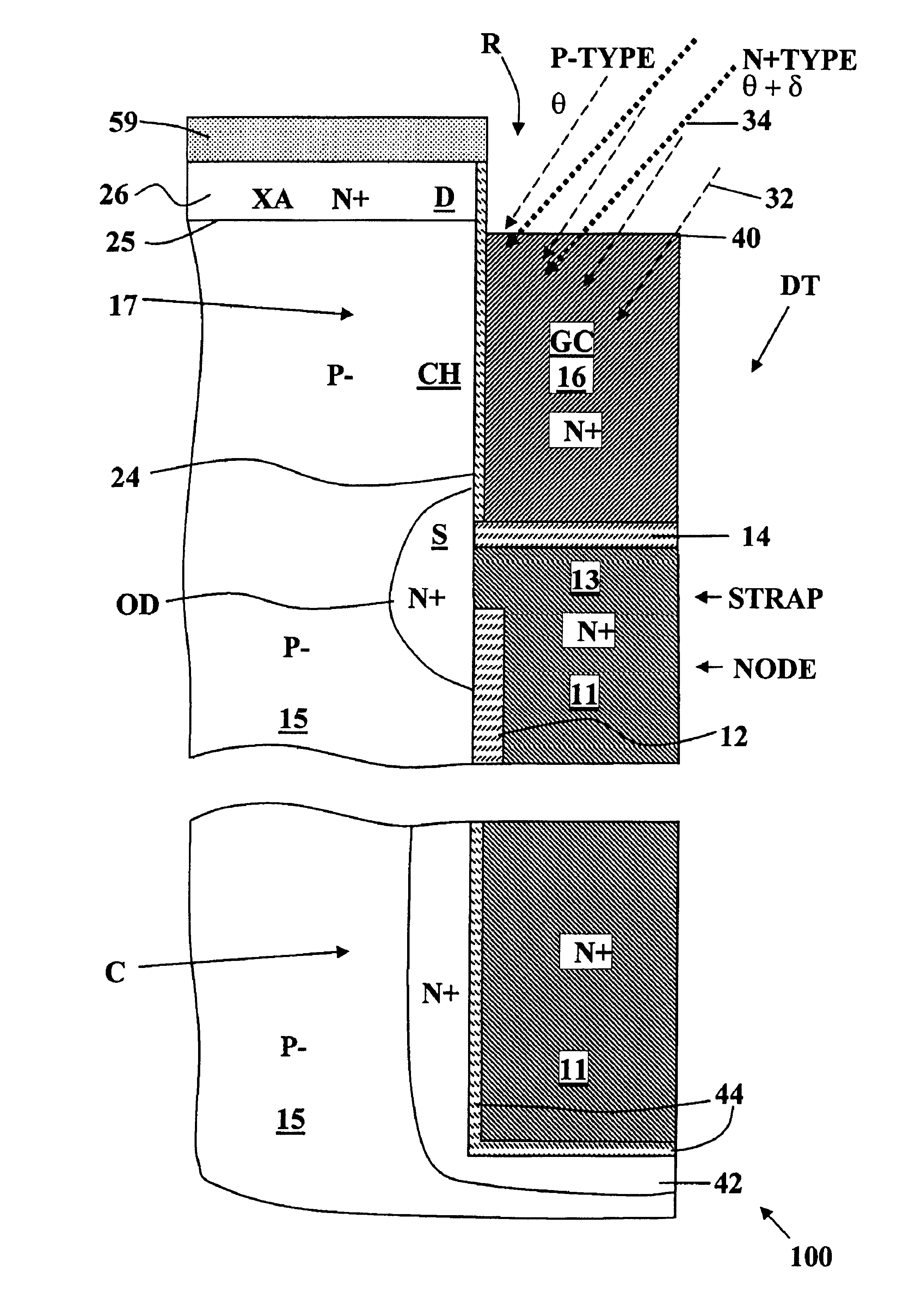
[0050]FIG. 3 illustrates a device structure and the Vt adjustment implant process in accordance with this invention with the N+ doped bit line diffusion XA region 26 shown at the top of the semiconductor substrate 15 while angled ion implantations 32 and 34 are being performed. It is possible that the XA region 26 is formed later in the manufacturing process, but the resulting channel doping levels are the same.

[0051]In accordance with this invention, the solution to the problem of FIGS. 2C and 2E is illustrated by FIG. 3 in which a Vt adjustment by an angled ion implantation of P-type dopant 32 has been provided into the recessed gate electrode 16 composed on N+ doped polysilicon implanted at the lesser angle θ with respect to vertical and the lateral scattering of the energetic ions combined with diffusion creates a laterally graded profile as illustrated by dopant profile 18P″ or 18P″ in FIG. 2C combined with an implant of N-type dopant ions 34 at a greater angle θ+δ with respect...


PUM


Abstract

A method of formation of a deep trench vertical transistor is provided. A deep trench with a sidewall in a doped semiconductor substrate is formed. The semiconductor substrate includes a counterdoped drain region in the surface thereof and a channel alongside the sidewall. The drain region has a top level and a bottom level. A counterdoped source region is formed in the substrate juxtaposed with the sidewall below the channel. A gate oxide layer is formed on the sidewalls of the trench juxtaposed with a gate conductor. Perform the step of recessing the gate conductor below the bottom level of the drain region followed by performing angled ion implantation at an angle θ+δ with respect to vertical of a counterdopant into the channel below the source region and performing angled ion implantation at an angle θ with respect to vertical of a dopant into the channel below the source.

Description

BACKGROUND OF INVENTION[0001]This invention relates to the fabrication of Vertical Metal-Oxide-Semiconductor Field Effect Transistors (MOSFETs), which provide improved threshold variation and offer channel length scalability superior to devices existing in the prior art.[0002]In DRAM (Dynamic Random Access Memory) devices, a transfer MOSFET device is employed as a switch connected to the charge storing capacitor. A DRAM circuit usually includes an array of memory cells interconnected by rows known as wordlines and columns known as bitlines. Reading data from or writing data to a particular memory cell in the DRAM is achieved by simultaneously activating the combination of a selected wordline and a selected bitline. Different types of MOSFETs are used in DRAM circuits.[0003]FIG. 1A is a fragmentary, schematic, vertical sectional elevational view of a prior art vertical, deep trench, MOSFET, DRAM cell 10 formed in a P− doped silicon substrate 15. The cell 10 includes a vertical MOSFET...

Claims


Application Information

Patent Timeline
Patent Type & Authority Patents(United States)
IPC IPC(8): H01L21/02H01L21/70H01L21/336H01L21/8234H10B12/00
CPCH01L21/26586H01L27/10864H01L27/10876H01L29/1041H01L29/66537H01L29/66666H01L29/7827H01L29/945H10B12/0383H10B12/053H01L21/8234H01L21/18H01L29/732H10B99/00
Inventor WANG, GENGMCSTAY, KEVINWEYBRIGHT, MARY ELIZABETHLI, YUJUNCHIDAMBARRAO, DURESETI
Owner INFINEON TECH AG
Features
  • R&D
  • Intellectual Property
  • Life Sciences
  • Materials
  • Tech Scout
  • Unparalleled Data Quality
  • Higher Quality Content
  • 60% Fewer Hallucinations
Learn More