Bendable high flux LED array

a high-flux led array, bendable technology, applied in the direction of light-emitting devices, semiconductor devices for light sources, solid-state devices, etc., can solve the problems of degrading the flux performance & long-term reliability of led arrays, the led array does not have features particularly suitable for 3 dimensional configurations, and the 3 dimensional configurations can fit inside the housing with interior curvature, etc., to achieve the effect of being easily variabl

Active Publication Date: 2005-08-30
EPISTAR CORP
View PDF15 Cites 653 Cited by
  • Summary
  • Abstract
  • Description
  • Claims
  • Application Information

AI Technical Summary

Benefits of technology

[0020]Each of the metal heat spreaders may be attached with a thermally conductive material to a metal base which functions as a heat sink. Because the electrical interconnection layer is bendable, the inventive LED array may be bent such that these heat spreaders can be attached to a curved surface on this base or to separate flat surfaces ...

Problems solved by technology

However, either approach increases the amount of heat generated by the LEDs, which potentially can degrade the flux performance & long term reliability of the LEDs.
Also such 3 dimensional configurations can fit inside housings with interior curvature not as suitable for coplanar LED arrays, such as some automobile housings for turn signals.
Typical LED lamps do not comprise special heat spreaders which allow this pyramid-shaped heat flow pattern away from the LED die.
Although this prior patent application discloses an LED array which enhances heat dissipation, such an LED array does not have features particularly suitable for 3 dimensional configurations.
If an LED array disclosed in this prior patent application is bent significantly into a 3 dimensional...

Method used


Image

  • Bendable high flux LED array
  • Bendable high flux LED array
  • Bendable high flux LED array

Examples


first embodiment

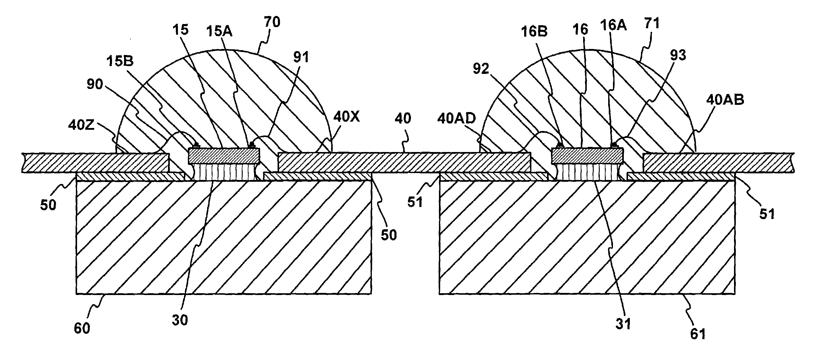
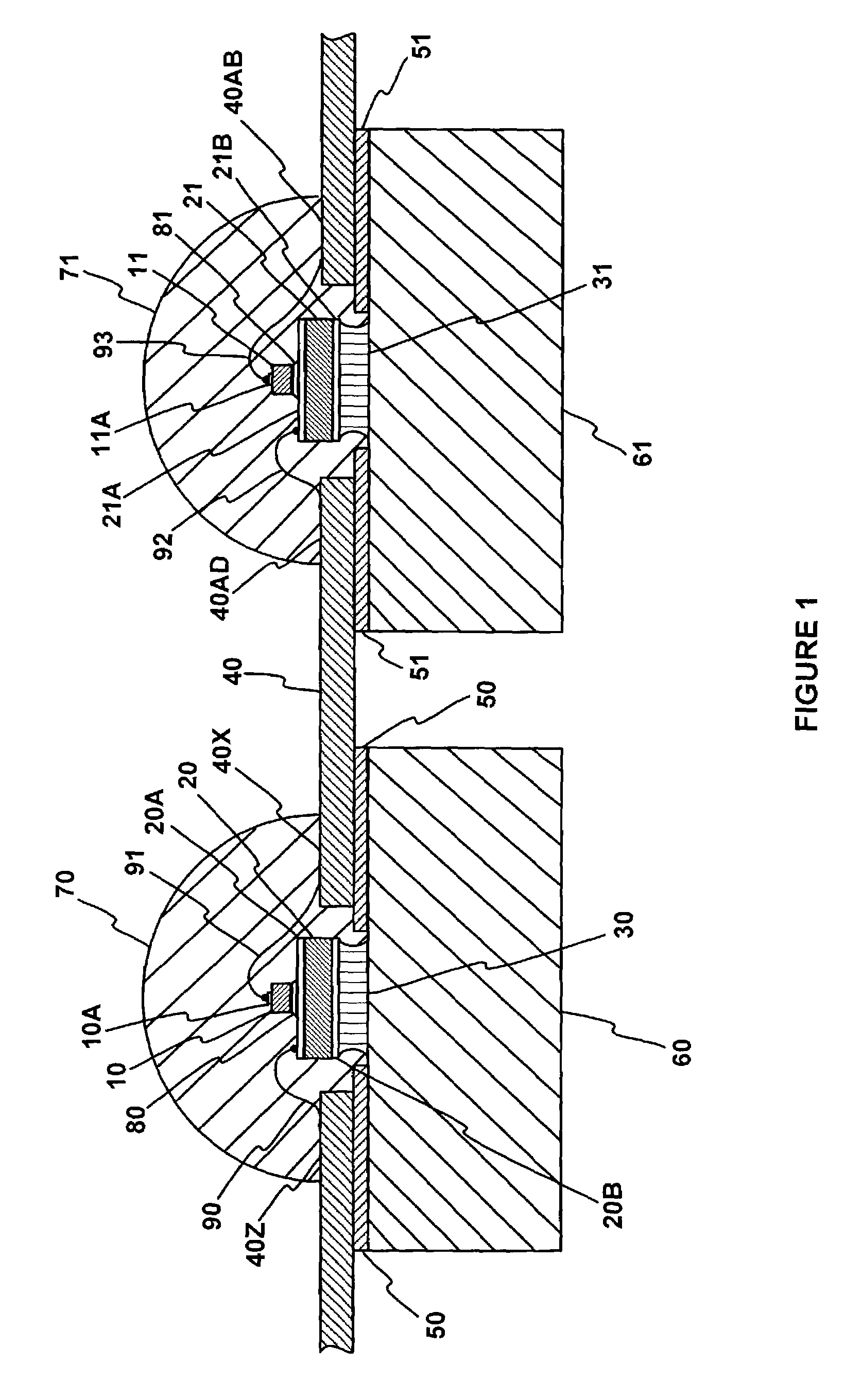
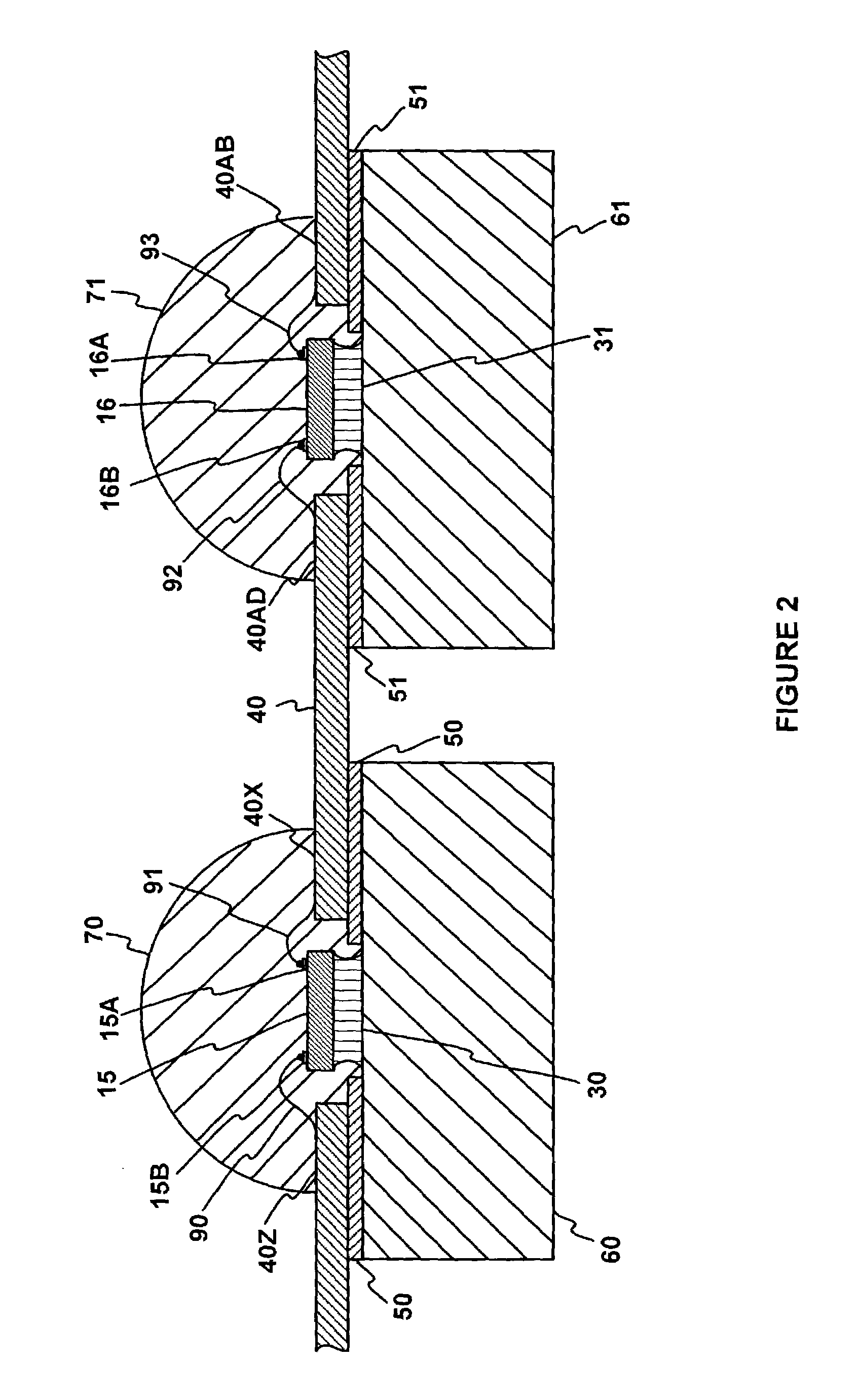
[0042]In the present invention (FIG. 1), an LED (light emitting diode die) array comprises a plurality of LEDs (e.g., LED 10 and LED 11) and a plurality of metal heat spreaders (e.g., metal heat spreader 60 and metal heat spreader 61). Some dielectric material (e.g., dielectric layer 50 and dielectric layer 51), such as epoxy, is disposed over each metal heat spreader in this LED array. A bendable electrical interconnection layer is disposed over the dielectric material on each metal heat spreader, and this dielectric material electrically insulates this electrical interconnection layer from each metal heat spreader. As shown in FIG. 1, this electrical interconnection layer may be a metal lead frame 40 with a plurality of stamped or etched metal pathways which electrically interconnect all LEDs in series, in parallel, in anti-parallel, or in some combination of these circuit configurations. This lead frame's metal pathways are electrical current pathways which carry electricity to t...

eighth embodiment

[0060]In the present LED array, each heat spreader (e.g., metal pathway 43W) is electrically isolated from adjacent metal pathways (e.g., metal pathway 43Z and metal pathway 43X) that are electrically coupled to the corresponding LED (e.g., flip chip LED 150). In other embodiments, each heat spreader may be a metal pathway that is electrically coupled to a corresponding LED. For example, LED submount 140 may be disposed with both thermal contact 140G and bottom electrical contact 140B above leadframe heat spreader 43W. A thermally and electrically conductive material, such as solder or silver-filled epoxy, may structurally couple these two submount contacts to lead frame heat spreader 43W. In this configuration, each metal heat spreader (e.g., metal pathway 43W, metal pathway 43AA) is structurally and electrically integrated with a corresponding electrical current pathway (e.g., metal pathway 43CA, which may be a thermal pathway and also a cathode or anode bus for LEDs electrically ...

tenth embodiment

[0063]In one variation of the tenth embodiment, each heat spreader's base may be sufficiently large that a portion of it is disposed underneath both corresponding electrical current pathways. In this configuration, some of the dielectric body's molding compound is disposed between the bottom of one corresponding electrical current pathway (e.g., metal pathway 44Z) and the top of the corresponding heat spreader's base. Thus the molding compound in the dielectric body forms a dielectric layer between one correspond electrical current pathway and the underlying portion of the corresponding heat spreader, whereby the heat spreader and that electrical current pathway are electrically isolated from each other. In other embodiments of the present invention, some material in each dielectric body provides dielectric layer(s) disposed between portions of multiple corresponding electrical current pathways and underlying portions of the corresponding heat spreader. Such dielectric layers may be...


PUM


Abstract

A bendable light emitting diode (LED) array in accordance with the present invention includes heat spreaders, dielectric material disposed above each heat spreader, and a bendable electrical interconnection layer disposed above these heat spreaders and electrically insulated from these heat spreaders by the dielectric material. At least one via passes through the dielectric material above each heat spreader, and at least one LED die is disposed above each via. The bendable electrical interconnection layer may be a lead frame comprising metal pathways that electrically interconnect some or all LED dice in series, in parallel, in anti-parallel, or in some combination of these configurations. Each via contains a thermally conductive material in thermal contact with the corresponding heat spreader below it and in thermal contact with the corresponding LED die above it. The LED dice may be thermally and electrically coupled to submounts disposed above corresponding heat spreaders in some embodiments.

Description

[0001]This application claims the benefit of U.S. Provisional Application No. 60 / 348,500, filed on Jan. 16, 2002.BACKGROUND INFORMATION[0002]1. Field of the Invention[0003]The present invention relates to light emitting diodes and more particularly to arrays of light emitting diodes.[0004]2. Description of the Related Art[0005]Arrays of light emitting diodes (LED) may be utilized in a variety of high flux applications such as street lighting, traffic signals, automobile turn signals and brake lights. One way to enhance the performance of such LED arrays is to increase the flux produced per unit area of the LED array. To increase the flux per unit area, the spacing between LEDs in the array can be decreased and / or the flux produced by each individual LED can be increased. However, either approach increases the amount of heat generated by the LEDs, which potentially can degrade the flux performance & long term reliability of the LEDs. Thus, what is needed is a high flux LED array that...

Claims


Application Information

Patent Timeline
IPC IPC(8): H01L29/04H01L29/18H01L31/18H01L29/02H01L29/22H01L29/15H01L31/036H01L31/0376H01L31/20F21K99/00H01L33/62
CPCF21K9/00H01L33/62H01L2224/48091H01L2924/01078H01L2924/01079H01L2924/00014H01L2924/12041H01L2224/48465H01L2224/73265H01L2924/00012H01L2924/00H01L2224/16225H01L2224/32245H01L2924/181H01L2924/19107
Inventor HARRAH, SHANE
Owner EPISTAR CORP
Why Eureka
Try Eureka