Optical switch having photonic crystal structure

a technology of optical switches and crystal structures, applied in the field of optical switches, can solve the problems of limited operating wavelength range, interference with high-density integration, and difficulty in achieving high-speed swiching as high as 10 gbps or more, and achieve the effect of altering the refractive index

Inactive Publication Date: 2005-08-30
NEC CORP
View PDF17 Cites 75 Cited by
  • Summary
  • Abstract
  • Description
  • Claims
  • Application Information

AI Technical Summary

Benefits of technology

[0027]In yet another aspect of the invention, the photonic crystal structure comprises: means for refracting light by making incident light to be oblique with respect to the intrinsic axis of the photonic crystal; and means for altering the refractive index of the photonic crystal. The refractiv

Problems solved by technology

However, directly controlling on and off of the output of the semiconductor laser deteriorates oscillation stability of the semiconductor laser and above all high-speed swiching as high as 10 Gbps (giga-bits/second) or more is difficult to achieve.
However, the number of materials that can be selected by their intrinsic properties such as band-gap energy is limited, which results in limited operating wavelength range.
Therefore, in order to obtain sufficiently large difference between the signal light intensities of ON and OFF states, the length of the optical path needs to be as long as about several-hundreds of microns, which interf

Method used


Image

  • Optical switch having photonic crystal structure
  • Optical switch having photonic crystal structure
  • Optical switch having photonic crystal structure

Examples


first embodiment

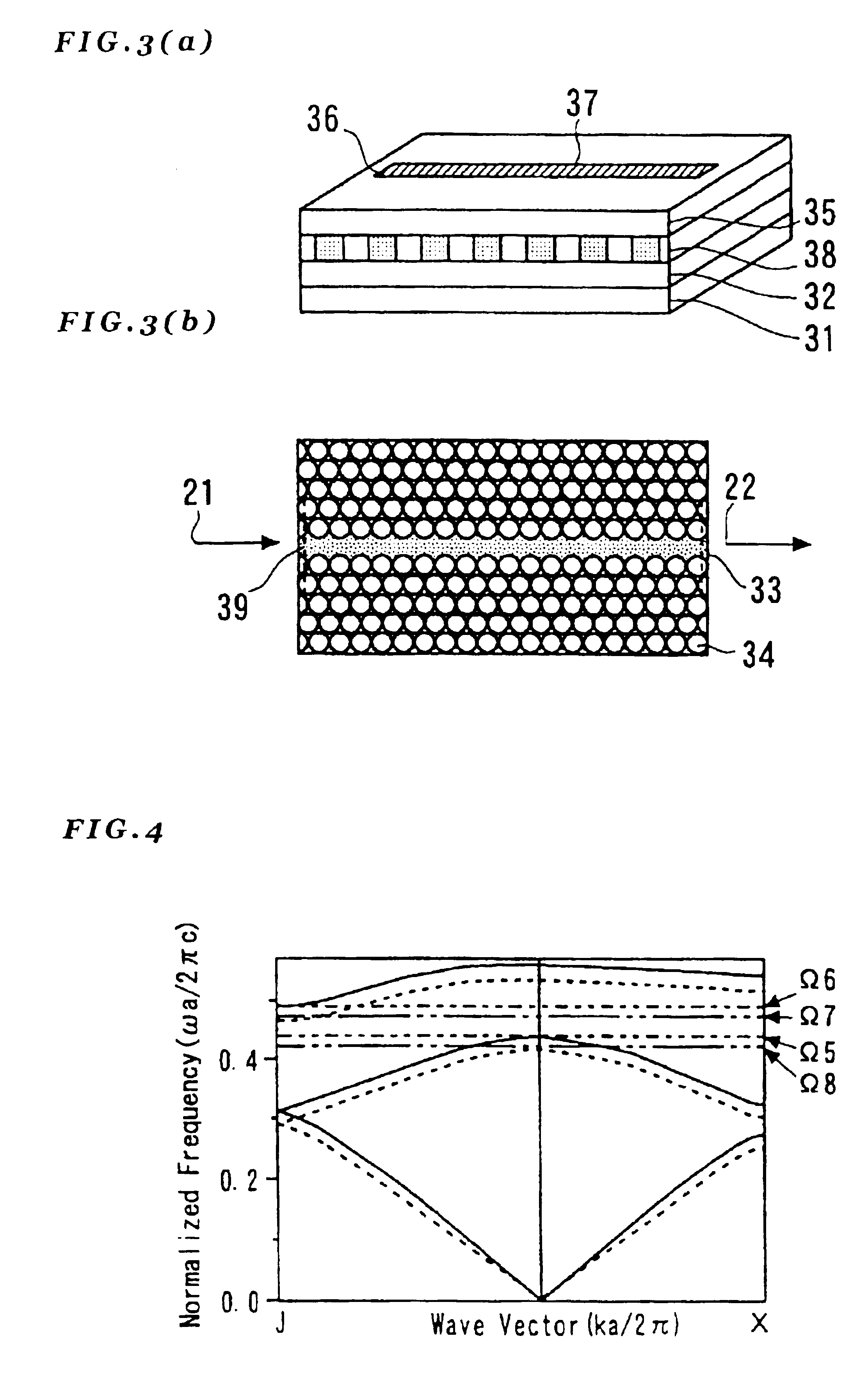
[0045]Hereinafter, embodiments of the present invention will be described with reference to the drawings. FIG. 3A is a schematic view showing a structure of the invention, and FIG. 3B is a plan view showing a photonic crystal layer 38.

[0046]Referring to FIG. 3A, an n-type semiconductor clad layer 32, and the photonic crystal layer 38 including i-type semiconductors 33 (base medium) and 34 having different refractive indices are formed on an n-type substrate 31 in this order.

[0047]A p-type semiconductor clad layer 35 is further provided on the photonic crystal layer 38, together with an electrode 36 and a lead wire 37 for current injection. The n-type substrate 31 is held at ground potential.

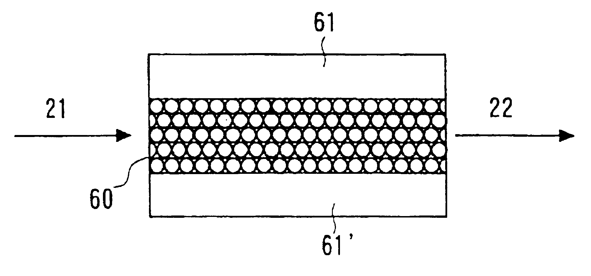
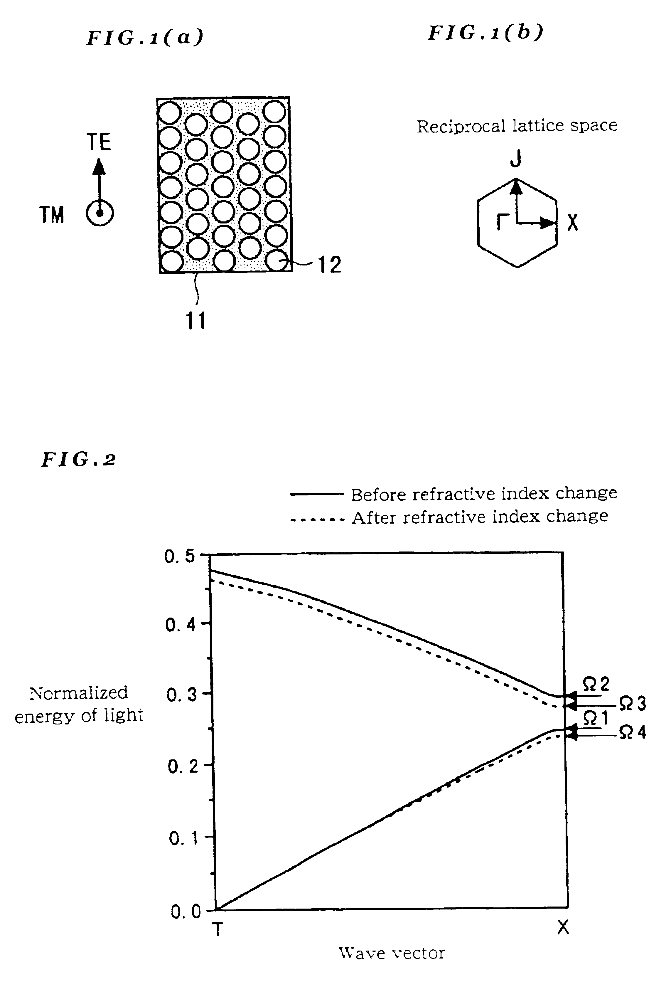
[0048]The i-type semiconductor (base medium) 33 is imbedded with cylinders made of the i-type semiconductor 34 in a two-dimensional triangular lattice (to have a alternately structure). There is a linear region where a row of the i-type semiconductor 34 is replaced with the base medium 33 in a di...

second embodiment

[0069]FIG. 12 is a top perspective view showing the structure of the invention shown in FIG. 11. The i-type, n−-type or p−-type semiconductor core layer 76 has a photonic crystal structure and is provided with a line-defect optical waveguide 77.

[0070]On both sides of the line-defect optical waveguide 77, an n-type region 78 and a p-type region 79 are provided, each having an n-type ohmic electrode 80 and a p-type ohmic electrode 81, respectively.

[0071]The operation principle of the second embodiment of the invention is the same as that of the first embodiment. Specifically, energy of the optical signal to be switched is within the photonic band gap of the slab photonic crystal. The line-defect optical waveguide formed in the photonic crystal has a propagation mode in the photonic band gap prior to current injection or voltage application to the electrodes.

[0072]When current is injected or a reverse bias voltage is applied between the electrodes 80 and 81, the photonic band structure...

fourth embodiment

[0082]Next, operation principle of the invention will be described. The incident light 21 is split at a Y-shaped junction of the line-defect waveguide to be transmitted through two optical paths 40 and 40′ as upper and lower branches. The beams that propagate through the two optical paths are recombined at the other Y-shaped junction and output as emitted light 22. Since the lengths of the optical paths of the upper and lower branches are equal when no current is injected, the phase difference between the two branched beams is zero (in-phase), and thus the intensity of the output light 22 (which is the coherent light of the recombined beams) is the maximum. Even when the lengths of the two optical paths are different, the phase difference is equivalent to zero as long as the difference between the lengths of the optical paths is a multiple of the wavelength.

[0083]When a current is injected through at least one of the electrodes of the upper and lower branches to alter the refractive...


PUM


Abstract

The present invention provides an optical switch having a photonic crystal structure.
An optical switch of the invention has a slab optical waveguide structure whose core (35) has a two-dimensional photonic crystal structure where two or more media (33, 34) with different refractive indices are alternately and regularly arranged in a two-dimensional manner. The photonic crystal structure comprises: a line-defect waveguide; and means for altering the refractive index of the line-defect waveguide.

Description

FIELD OF THE INVENTION[0001]The present invention relates to an optical switch. More particularly, the present invention relates to an optical switch having a photonic crystal structure.BACKGROUND OF THE INVENTION[0002]Optical communication requires a mechanism for switching optical signals on and off in accordance with binary signals (i.e., 0 or 1). One of the simplest mechanisms is to directly control on and off of output of a semiconductor laser used as a light source. However, directly controlling on and off of the output of the semiconductor laser deteriorates oscillation stability of the semiconductor laser and above all high-speed swiching as high as 10 Gbps (giga-bits / second) or more is difficult to achieve.[0003]Another technique for controlling on and off of an optical signal is to use an optical switch. According to this technique, constant optical outputs from a semiconductor laser are modulated to be on and off by a device provided at a subsequent stage. This device is ...

Claims


Application Information

Patent Timeline
IPC IPC(8): G02F1/01G02F1/025G02B6/122G02B6/12G02F1/015G02F1/313
CPCB82Y20/00G02B6/1225G02F1/025G02F2202/32G02F2203/48
Inventor SHIRANE, MASAYUKITOKUSHIMA, MASATOSHI
Owner NEC CORP
Why Eureka
Try Eureka