

Method for fabricating a filament affixed trace within an electronic device
- Summary
- Abstract
- Description
- Claims
- Application Information
AI Technical Summary
Benefits of technology
Problems solved by technology
Method used
Image

Examples
Embodiment Construction
[0027]One embodiment of the present invention consists essentially of replacing common dielectric substrates in which conductive traces are embedded within multi-layer circuit boards and other microelectronic devices with air. As shown in Table 1, above, dry air has an extremely low loss tangent and relative permittivity with respect to the other various solid substances listed in Table 1. Dry air is a close approximation, with respect to attenuation coefficient αD, to the vacuum, which has an attenuation coefficient αD of zero. The inventors realized that if common solid dielectric substrates can be economically replaced with air within multi-layer circuit boards and other microelectronic devices, the usable signal frequency range within traces incorporated into those circuit boards and microelectronic devices can be greatly expanded while maintaining signal intensity attenuation below required threshold values.
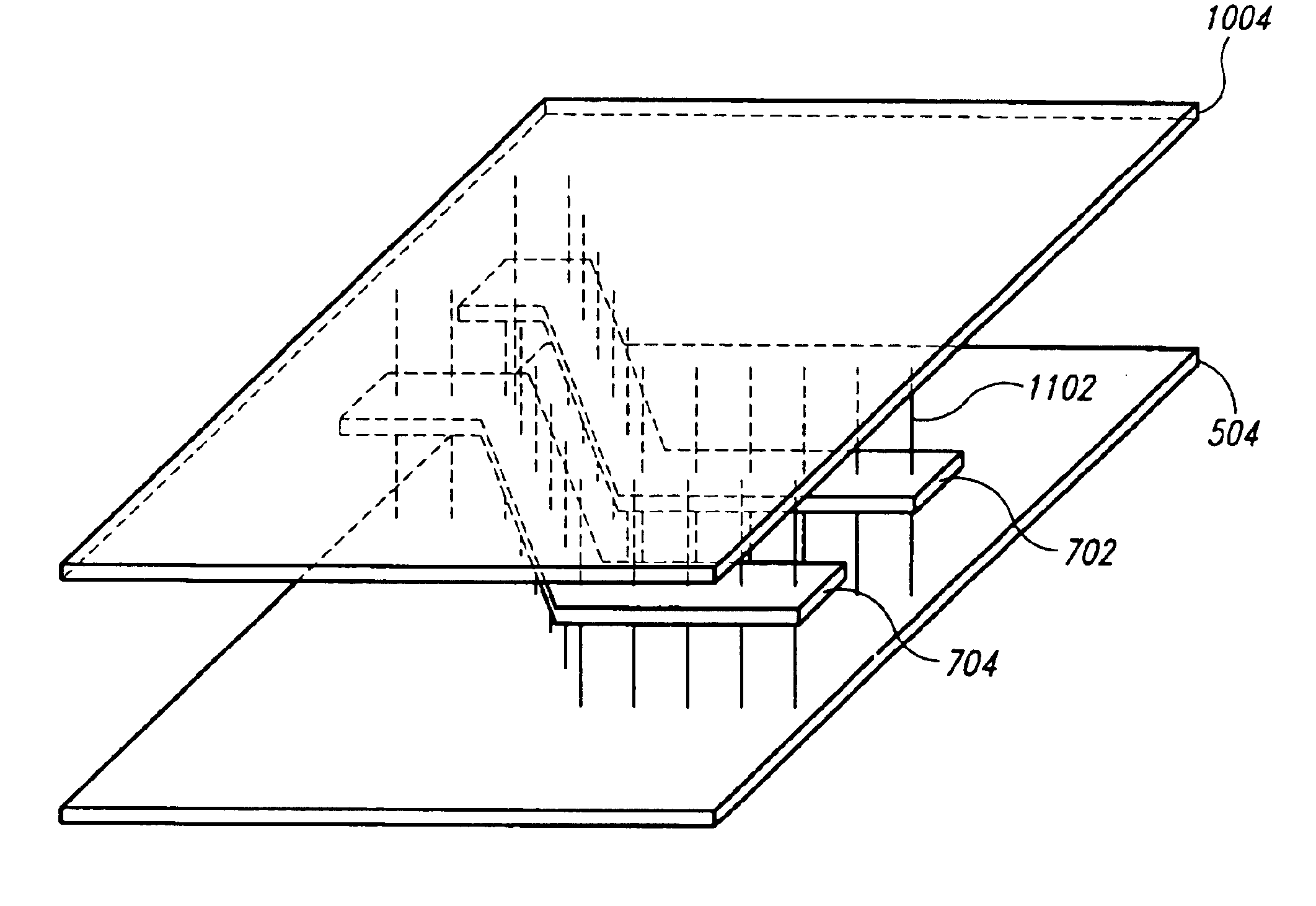
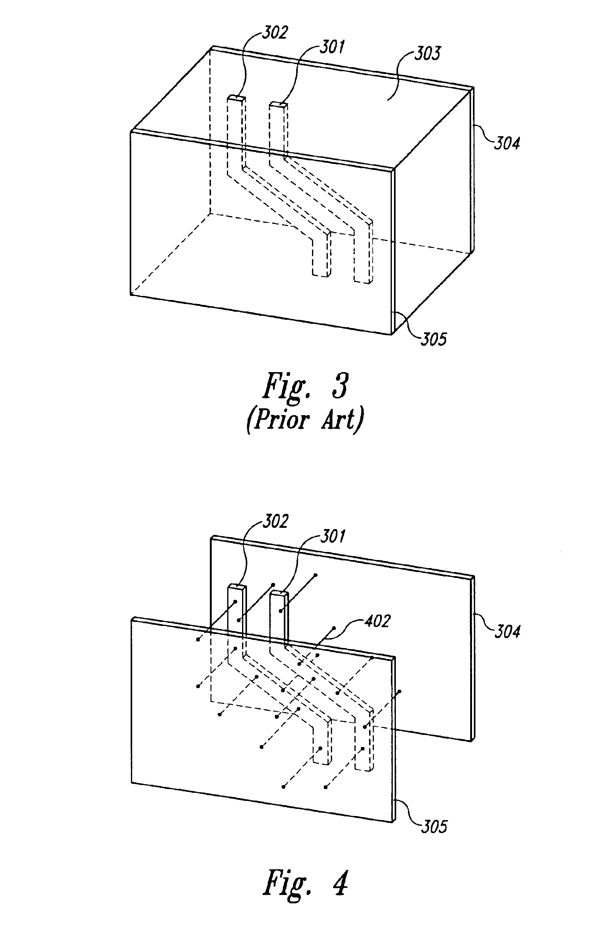
[0028]FIG. 4 illustrates the present invention employed within a portio...
PUM
| Property | Measurement | Unit |
|---|---|---|
| Fraction | aaaaa | aaaaa |
| Angle | aaaaa | aaaaa |
| Electrical conductor | aaaaa | aaaaa |
Abstract
Description
Claims
Application Information