

High-capacitance density thin film dielectrics having columnar grains formed on base-metal foils
a technology of thin film dielectrics and columnar grains, which is applied in the direction of thin/thick film capacitors, fixed capacitor details, fixed capacitors, etc., can solve the problems of microprocessor voltage drop or power droop, and the need to supply sufficient current to accommodate the faster circuit switching becomes an increasingly important problem, and achieves high capacitance densities and low loss tangents. , the effect of high capacitance density
- Summary
- Abstract
- Description
- Claims
- Application Information
AI Technical Summary
Benefits of technology
Problems solved by technology
Method used
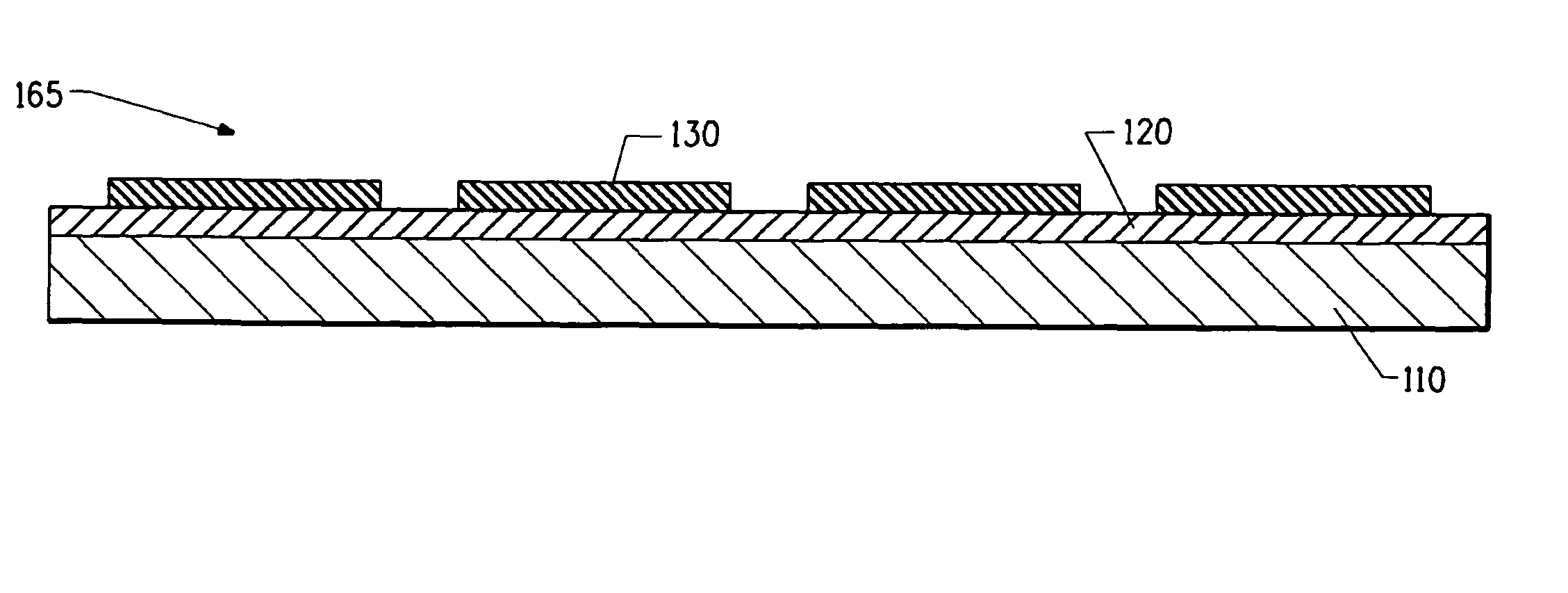
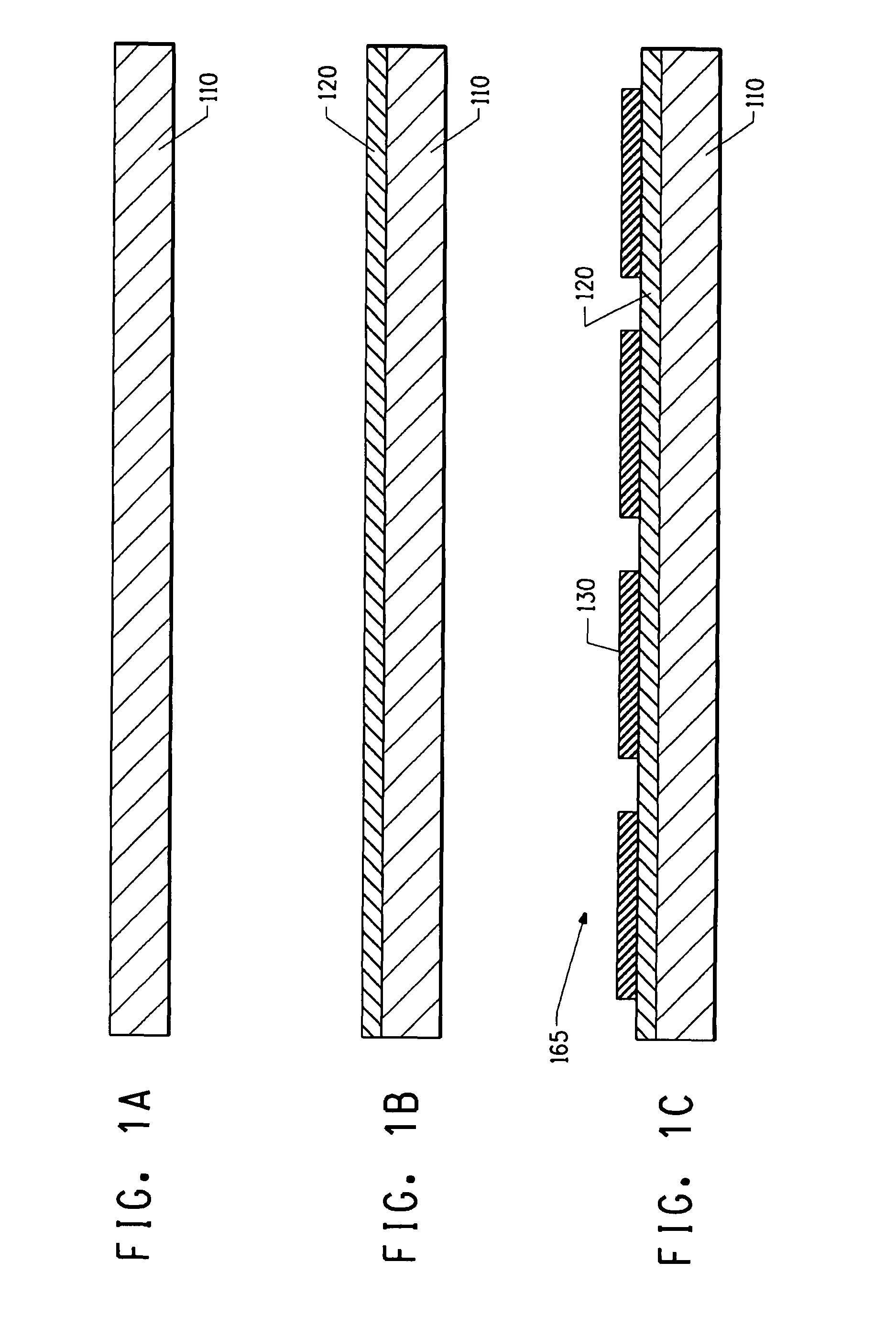
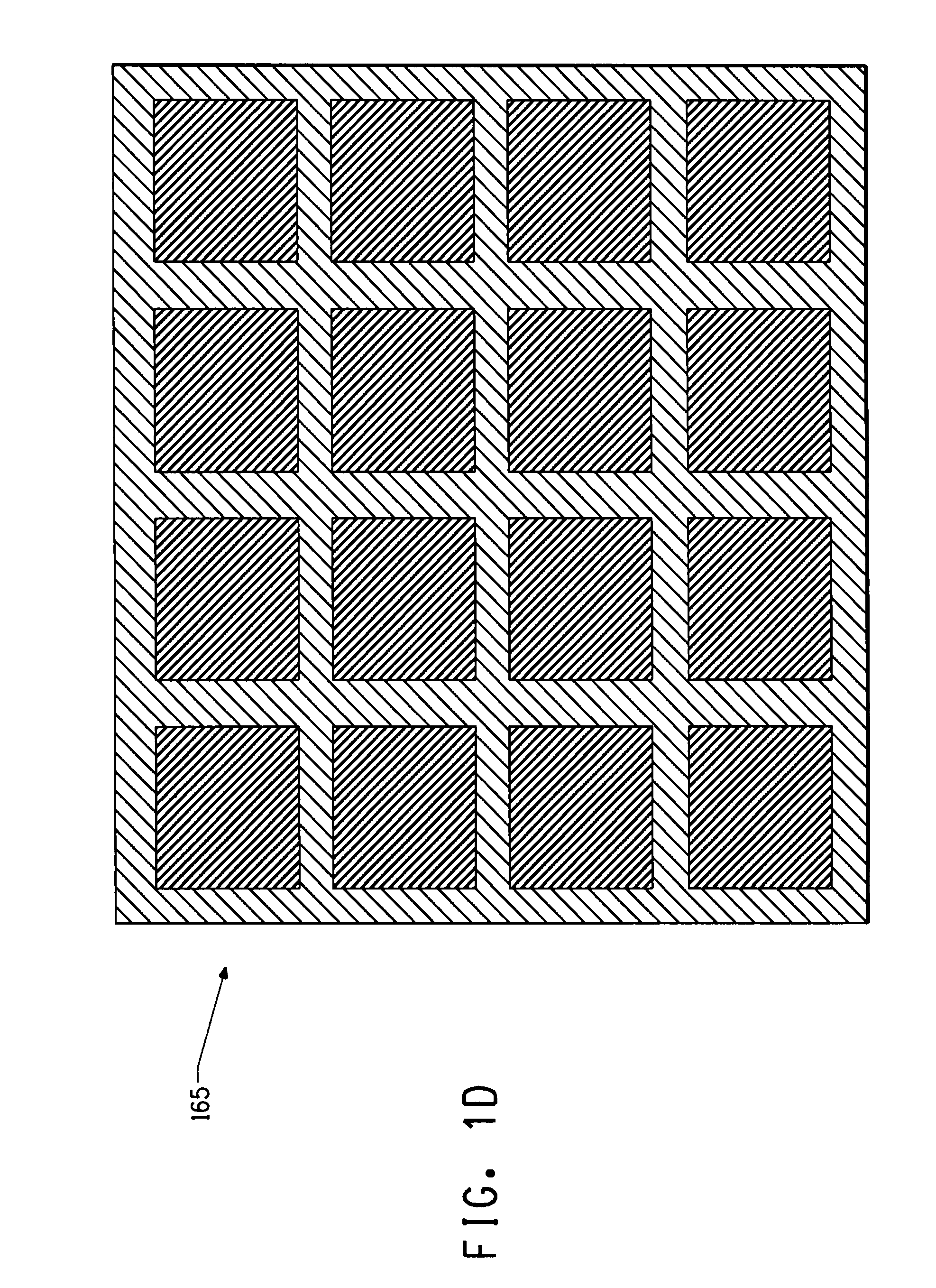
Image

Examples
example 1
[0040]A 76.2 micron thick 201 type nickel foil obtained from All Foils Inc. was cut to a size of 62 mm by 62 mm and ultrasonically cleaned with acetone for 5 minutes followed by an ultrasonic rinse with a mix of de-ionized water and industrial propyl alcohol. The nickel foil was then annealed at 1000° C. for a period of 90 minutes at peak temperature under a partial pressure of oxygen of between 10−14 to 10−15 atmosphere. This atmosphere was accomplished by use of a mixture of forming gas (1% hydrogen in nitrogen) and nitrogen. The annealing induced grain growth in the metal foil. After annealing, many grains of the nickel extended across the entire thickness of the foil so that they were substantially equal in size to the thickness of the foil.
[0041]The annealed nickel foil was polished using a chemical mechanical polishing process to a mirror finish. After polishing, the foil was ultrasonically cleaned for 5 minutes in acetone followed by an ultrasonic rinse in a mix of de-ionized...
PUM
| Property | Measurement | Unit |
|---|---|---|
| thickness | aaaaa | aaaaa |
| thickness | aaaaa | aaaaa |
| temperature | aaaaa | aaaaa |
Abstract
Description
Claims
Application Information