Semiconductor device testing contactor having a circuit-side contact piece and test-board-side contact piece

a technology of contactor and semiconductor, which is applied in the direction of semiconductor/solid-state device testing/measurement, coupling device connection, instruments, etc., can solve the problems and high cost of contactor, and achieve the effect of short life duration, short life duration and high cos

Inactive Publication Date: 2005-09-06
SOCIONEXT INC
View PDF8 Cites 31 Cited by
  • Summary
  • Abstract
  • Description
  • Claims
  • Application Information

AI Technical Summary

Benefits of technology

[0031]It is a general object of the present invention to provide an improved and useful contactor for testing a semiconductor device in which contactor the above-mentioned problems are eliminated.
[0032]A more specific object of the present invention is to provide a contactor for testing a semiconductor device which contactor, for a wafer-level burn-in test: (1) is low-cost and can have a multitude of probes; (2) can be replaced independently of other contactors when a probe thereof is damaged; and (3) has high heat resistivity and a mechanical life duration of several hundreds of times, and which contactor, for a final test: (1) can undergo a high-speed test due to its short probe; and (2) can be replaced independently of other contactors when a probe thereof is damaged, and a manufacturing method of the contactor.

Problems solved by technology

t has conventionally been very difficult to realize a contactor which fulfills these requirements, and if the contactor could be realized, the contactor would be extraordinarily costly and have a short life duration.
That is, since the length of the probe is substantially proportional to the impedance of the contactor, the high-speed test cannot be performed with the increased impedance of a contactor having a long probe.
It has conventionally been very difficult to realize a contactor which fulfills these requirements, and if it could be realized, the contactor would be extraordinarily costly.
Therefore, if a terminal-containing surface of an LSI circuit is not flat enough, the narrow range of the elastic deformation cannot provide a sure contact.
Thus, the LSI circuit has to have such a costly substrate as a ceramic substrate and a glass substrate having a flat enough surface.
Additionally, with respect to such an LSI circuit as a wafer-level CSP using large solder balls, heights of the solder balls on a wafer vary by approximately 100 μm, with which variation the anisotropic conductive rubber cannot provide a sure contact.
The anisotropic conductive rubber is extremely prone to deterioration in a high-temperature condition and, thus, cannot endure a repeated contact.
Especially in a high-temperature condition (ranging from 125° C. to 150° C.) as in a burn-in test, a base rubber undergoes a plastic deformation and, thus, cannot endure repeated use.
However, an anisotropic conductive rubber usable for the size of wafer costs tens of thousands of yen per piece, raising a test cost for a wafer to be tested.
The above-mentioned contactor using a spring pin has the following problems to be solved: (1) an extremely high manufacturing cost; and (2) an irreplaceable contact pin.
Therefore, in accordance with the number of probes to be formed, a manufacturing cost of a contactor increases.
In this case, a contactor has to have 50,000 probes correspondingly, extremely raising a manufacturing cost of the contactor.
Additionally, a life cycle of a contactor is currently shortened to approximately 180 days, inevitably putting limits to repeated use of a contactor used in a lengthy burn-in test.
Therefore, a depreciation expense of a contactor for a wafer becomes enormously high.
Hence, such a contactor cannot practically be employed.
When even only one of contact pins (probes) becomes damaged and unusable, the entire contactor also becomes unusable.
As a matter of fact, in an LSI circuit test, it is difficult to completely keep a contact pin from being burned by a latch-up (overcurrent) in a burn-in test or from being damaged by a mechanical shock.
However, since a contact pin is directly bonded to an electrode of a test board, it is difficult to remove a damaged pin from among other pins and re-form a new pin among the other pins.
Therefore, a loss of only one pin may lead to spoiling an entire contactor and losing a huge sum financially.
Also, the cantilever probing card has a problem to be solved: a high impedance.
With the probe card having the large impedance, a high-speed test cannot be performed.
However, a high-speed device designed to operate at more than 200 MHz cannot be tested at high speed because of the large impedance of the cantilever probing card.

Method used


Image

  • Semiconductor device testing contactor having a circuit-side contact piece and test-board-side contact piece
  • Semiconductor device testing contactor having a circuit-side contact piece and test-board-side contact piece
  • Semiconductor device testing contactor having a circuit-side contact piece and test-board-side contact piece

Examples


second embodiment

[0138]Next, a description will be given, with reference to FIG. 13, of the second embodiment according to the present invention.

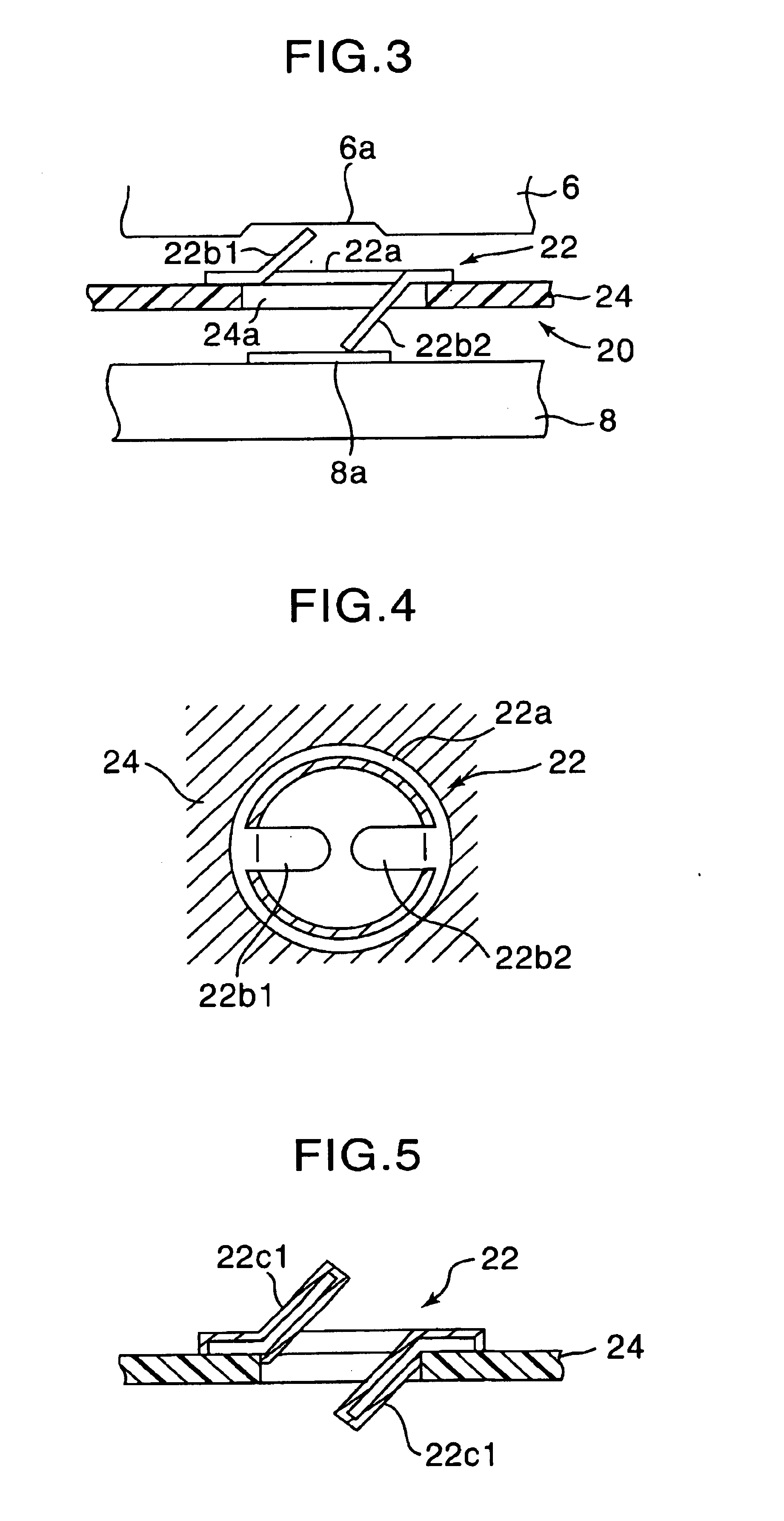
[0139]FIG. 13 is a cross-sectional view of a contact electrode 32 of a contactor according to the second embodiment of the present invention. An entire structure of the contactor is the same as the above-mentioned contactor 20 according to the first embodiment, so a description thereof will be omitted.

[0140]The contact electrode 32 shown in FIG. 13 is formed after a copper plate or a copper foil is applied on both surfaces of the insulating substrate 24. The contact electrode 32, as the contact electrode 22, has an annular portion 32a and an LSI-circuit-side contact piece 32b1. The annular portion 32a and the LSI-circuit-side contact piece 32b1 are formed of a copper plate or a copper foil applied on one side (the LSI circuit 6's side) of the insulating substrate 24. Accordingly, the annular portion 32a and the LSI-circuit-side contact piece 32b1 are formed...

third embodiment

[0145]The contact electrode 42 with an annular portion 42a, shown in FIG. 14, according to the present invention is a contact electrode adapted to a case where a terminal of the LSI circuit 6 is a protruding electrode 6b such as a solder bump (shown in FIG. 16). In order to prevent an LSI-circuit-side contact piece 42b1 from undergoing a permanent deformation due to a contact pressure with the solder bump 6b, the two LSI-circuit-side contact pieces 42b1 are juxtaposed on both sides of a central piece 42b2 and a centerline of the solder bump 6b, avoiding the center of the solder bump 6b. In FIG. 15, the LSI-circuit-side contact piece 42b1 is level, not bent toward the LSI circuit 6.

[0146]FIG. 16 is a cross-sectional view of the contact electrode 42 placed between the LSI circuit 6 and the test board 8. The LSI-circuit-side contact pieces 42b1, pressed by the solder bump 6b, are elastically deformed toward the test board 8, bent into the opening 24a. This elastic deformation provides ...

first embodiment

[0149]As the contact electrode 22 according to the present invention, the contact electrode 52 shown in FIG. 18 has an annular portion 52a, an LSI-circuit-side contact piece 52b1 and a test-board-side contact piece 52b2. However, the contact electrode 52 according to the present embodiment is formed as follows: forming an opening 24b having a shape corresponding to a shape of the contact electrode 52 in the insulating substrate 24 in advance; and forming a conductive film around a periphery of the opening 24b by such a method as plating or sputtering. That is, the contact electrode 52 itself is formed by such a method as plating or sputtering.

[0150]FIGS. 19A, 19B, and 19C illustrate steps of forming the contact electrode 52. First, as shown in FIG. 19A, the opening 24b having the shape corresponding to the shape of the contact electrode 52 is formed in the insulating substrate 24. Since the insulating substrate 24 is formed of such a resin sheet as a polyimide resin sheet, the openi...


PUM

PropertyMeasurementUnit
temperatureaaaaaaaaaa
thickaaaaaaaaaa
heightsaaaaaaaaaa

Abstract

A contactor is placed between a semiconductor device and a test board. A contact electrode of the contactor electrically connects the semiconductor device to the test board. The contact electrode is formed of a conductive layer provided on an insulating substrate. The contact electrode includes a first contact piece which contacts a terminal of the semiconductor device, a second contact piece which contacts an electrode of the test board, and a connecting portion which electrically connects the first contact piece and the second contact piece.

Description

BACKGROUND OF THE INVENTION[0001]1. Field of the Invention[0002]The present invention generally relates to a contactor for testing a semiconductor device and, more particularly, to a contactor for testing an LSI (Large Scale Integration) circuit having fine terminals or terminals arranged with a fine pitch and a manufacturing method of the contactor.[0003]In testing a semiconductor device such as an LSI circuit during a manufacturing process thereof, a contactor is used for making electrical contact with a terminal of the LSI circuit. In testing a conventional semiconductor device having a socket for connection, the socket can be used as a contactor. However, an LSI circuit, such as a so-called KGD (Known Good Die), which is to be tested as a bare chip not yet packaged, or a CSP (Chip Size Package), does not have a socket. Therefore, a contactor for test use needs to be prepared for such an LSI circuit.[0004]Recently, a wafer-level packaging technology has been developed, which tech...

Claims


Application Information

Patent Timeline
Patent Type & Authority Patents(United States)
IPC IPC(8): G01R1/04G01R1/02G01R1/073H05K3/32G01R31/26H01L21/66H01R11/01H01R33/76H01R43/00
CPCG01R1/0408G01R1/073H05K3/326Y10T29/49208Y10T29/49204Y10T29/49218Y10T29/49217Y10T29/49151H01L22/00
Inventor MARUYAMA, SHIGEYUKIMATSUKI, HIROHISA
Owner SOCIONEXT INC
Why Eureka
Try Eureka