Group III nitride compound semiconductor device and method of producing the same

Inactive Publication Date: 2005-09-06
TOYODA GOSEI CO LTD
View PDF15 Cites 22 Cited by
  • Summary
  • Abstract
  • Description
  • Claims
  • Application Information

AI Technical Summary

Benefits of technology

[0014]On the other hand, Japanese Patent Publication No. Hei. 5-86646 has disclosed the use of a buffer layer having a thickness of from 1000 Å to 7000 Å. The fact that the upper limit of the film thickness range

Problems solved by technology

According to the inventors' examination, there is a risk of the cracking in the first group III nitride compound layer or the second group III nitride compound semiconductor layer f

Method used


Image

  • Group III nitride compound semiconductor device and method of producing the same
  • Group III nitride compound semiconductor device and method of producing the same
  • Group III nitride compound semiconductor device and method of producing the same

Examples


Embodiment Construction

[0036]Respective elements of the present invention will be described below in detail.

Substrate

[0037]The material of a substrate is not limited specifically if a first group III nitride compound layer can be grown on the substrate. For example, sapphire, silicon, silicon carbide, zinc oxide, gallium phosphide, gallium arsenide, magnesium oxide, manganese oxide, group III nitride compound semiconductor single crystal, and so on, can be enumerated as substrate materials.

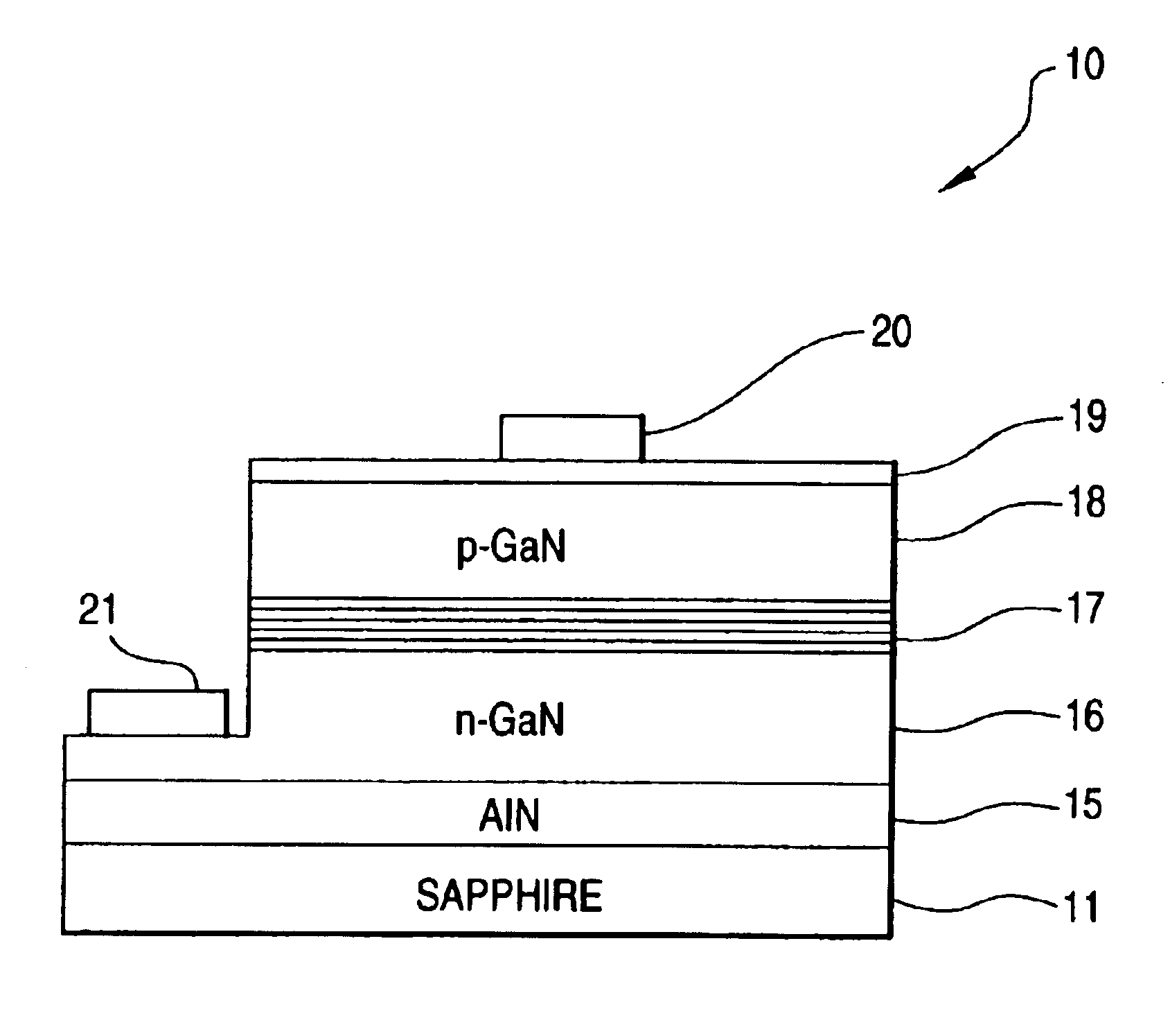
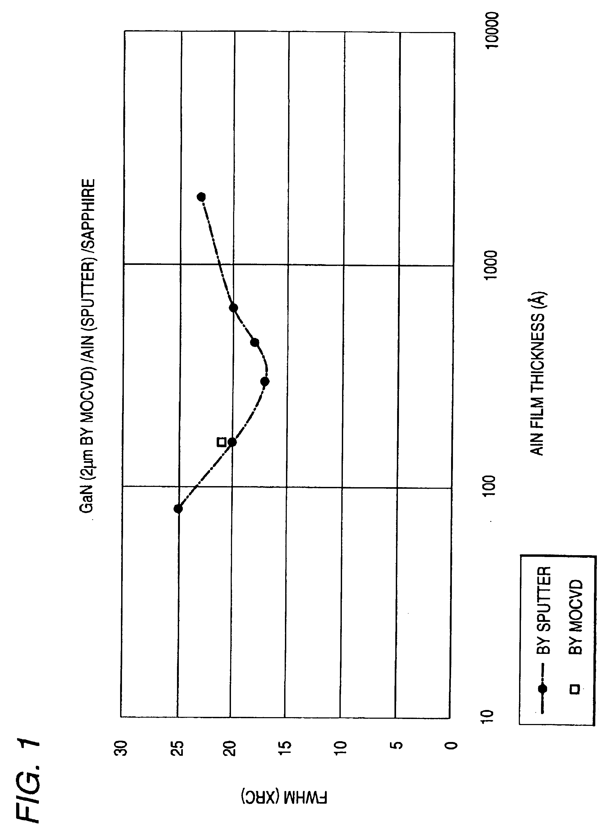
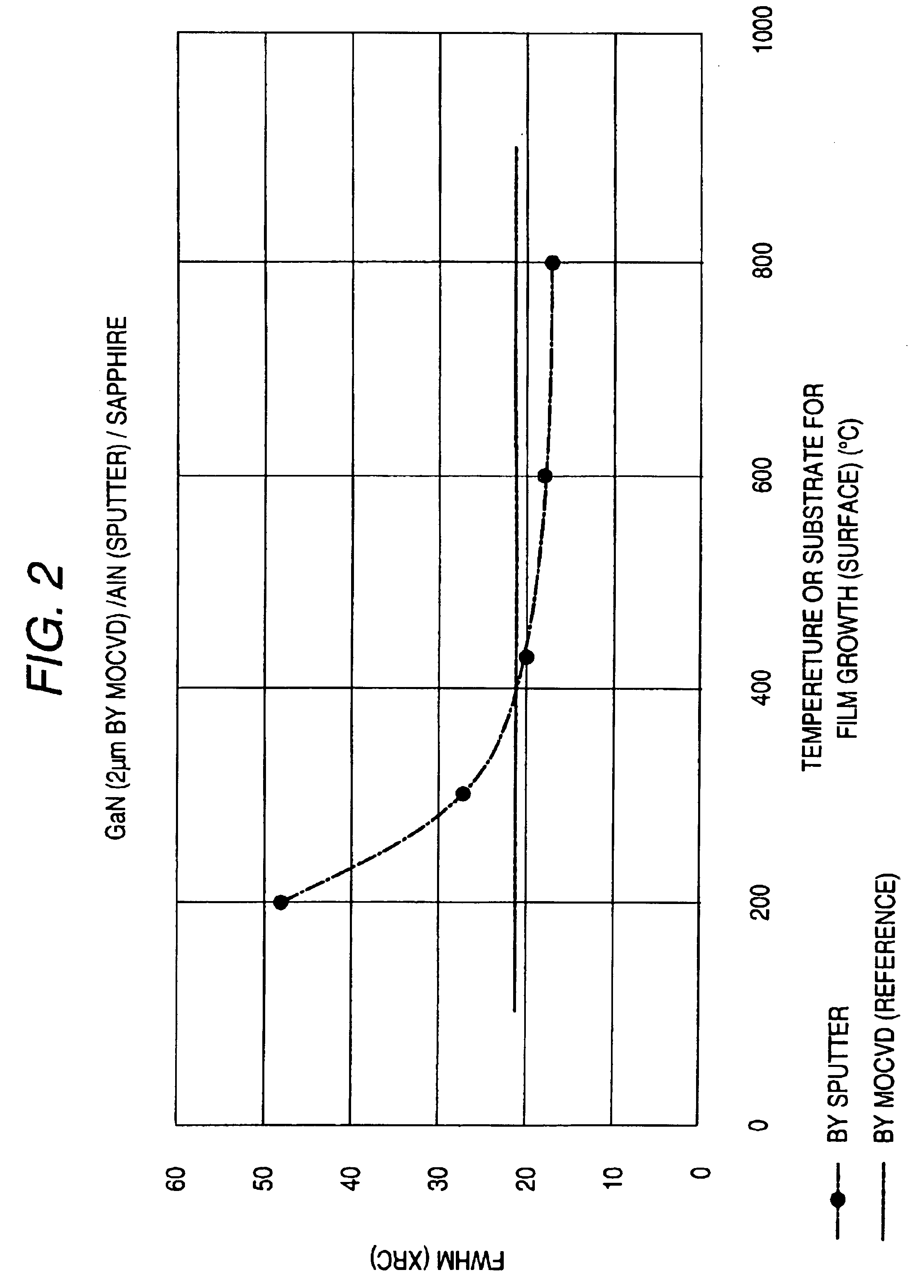
[0038]Of those materials, it is preferable to use a sapphire substrate and it is further preferable to use the face a of a sapphire substrate, (1120).

First Group III Nitride Compound Layer

[0039]A group III nitride compound or a group III nitride compound semiconductor is expressed by the general formula AlxGayIn1-x-yN (0≦X≦1, 0≦Y≦1, 0≦X+Y≦1), which includes so-called binary compounds such as AlN, GaN and InN, and so-called ternary compounds such as AlxGa1-xN, AlxIn1-xN and GaxIn1-xN, (0≦X≦1 in each formula). The group I...


PUM


Abstract

A first group III nitride compound layer, which is formed on a substrate by a method not using metal organic compounds as raw materials, is heated in an atmosphere of a mixture gas containing a hydrogen or nitrogen gas and an ammonia gas, so that the crystallinity of a second group III nitride compound semiconductor layer formed on the first group III nitride compound layer is improved. When the first group III nitride compound layer is formed on a substrate by a sputtering method, the thickness of the first group III nitride compound layer is set to be in a range of from 50 Å to 3000 Å.

Description

[0001]The present Application is a Divisional Application of U.S. patent application Ser. No. 09,516,177, filed on Mar. 1, 2000 now U.S. Pat. No. 6,713,789.BACKGROUND OF THE INVENTION[0002]1. Field of the Invention[0003]The present invention relates to a group III nitride compound semiconductor device and a method of producing the same.[0004]The present application is based on Japanese Patent Applications No. Hei. 11-130475 and 11-266499, which are incorporated herein by reference.[0005]2. Description of the Related Art[0006]A group III nitride compound semiconductor device such as a blue light-emitting device, or the like, was produced by the steps of: growing a buffer layer of AlxGa1-xN (0≦X≦1) on a sapphire substrate by a metal organic chemical vapor deposition method (abbreviated as “MOCVD method” in this specification); and further growing a group III nitride compound semiconductor layer on the buffer layer by the same MOCVD method.[0007]In the MOCVD method, an ammonia gas and ...

Claims


Application Information

Patent Timeline
IPC IPC(8): C30B25/02H01L21/02H01L21/205H01L33/00
CPCC30B25/02C30B29/403C30B29/406H01L21/0237H01L21/0242H01L21/02458H01L21/0254H01L21/02573H01L21/0262H01L21/02631H01L33/007B65F1/14B65F2210/104B65F2210/132
Inventor SHIBATA, NAOKIITO, JUNCHIYO, TOSHIAKIASAMI, SHIZUYOWATANABE, HIROSHISENDA, MASANOBUASAMI, SHINYA
Owner TOYODA GOSEI CO LTD
Why Eureka
Try Eureka