Dual-oxide transistors for the improvement of reliability and off-state leakage

a dual-oxide transistor and transistor technology, applied in the direction of transistors, semiconductor devices, electrical equipment, etc., can solve the problems of excessive forward and reverse gate leakage current, off-state leakage current, and small amount of unwanted leakage current, so as to reduce leakage current, minimize leakage current, and reduce the effect of leakage curren

Inactive Publication Date: 2005-10-04
ALTERA CORP
View PDF19 Cites 8 Cited by
  • Summary
  • Abstract
  • Description
  • Claims
  • Application Information

AI Technical Summary

Benefits of technology

[0013]In one embodiment of the present invention, a MOSFET has a thicker gate oxide at one or more ends of the gate, thereby minimizing leakage currents without adversely impacting overall device Vt as would occur if the gate oxide were made uniformly thicker.
[0014]The present invention also includes a method for fabricating a MOS transistor where the gate oxide is thicker at the ends of the gate for the purposes of reducing off-state leakage, increasing reliability and enhancing overall device performance. In one embodiment of the present invention, the MOS transistor is fabricated on a semiconductor substrate together with other devices in an integrated circuit (IC), using conventional IC fabrication steps. With some modification of one or more masks in the conventional IC processing steps, a nonuniform gate oxide is created that is thicker near the ends of the conducting channel of MOS transistor. Therefore, the present invention provides a MOS transistor with reduced leakage currents, and does not require additional complicated manufacturing steps for making the MOS transistor.

Problems solved by technology

In practice, however, there is typically a small amount of unwanted leakage current when device 10 is off.
There are several causes of off-state leakage currents.
Parasitic leakage paths between the gate and channel, commonly referred to as sidewall leakage, can result in excessive forward and reverse gate leakage currents.
Devices which exhibit high edge conduction and sidewall leakage are characterized by degraded device performance, such as increased off-state power dissipation.
For example, in practice processing steps associated with the formation of shallow trench isolation (STI) may result in electrons being trapped near a substrate-nitride interface, inducing sidewall leakage between an isolating trench and a device.
The lower threshold voltage, Vt, means higher off-state leakage currents that increase overall power consumption, result in excess heat generation and can cause problems related to the dissipation of excess heat.
Gate oxide thinning occurs over the device lifetime due to stresses on the device such as high applied voltage levels, temperature and imperfections in the oxide layer.
The phenomenon of the thinning of the gate oxide film increases the likelihood of dielectric breakdown which an adversely affect the operating characteristics of devices.
Moreover, the well-known “hot-carrier effect” can cause damage to the oxide layer by increasing the chances of oxide breakdown, particularly at oxide edges.
Particularly in low power or high temperature applications, leakage currents can represent a significant source of device degradation and performance impairment.
Such failure analysis projects are costly and highly dependent upon the skills and resourcefulness of the individuals conducting the failure analysis.

Method used


Image

  • Dual-oxide transistors for the improvement of reliability and off-state leakage
  • Dual-oxide transistors for the improvement of reliability and off-state leakage
  • Dual-oxide transistors for the improvement of reliability and off-state leakage

Examples


Embodiment Construction

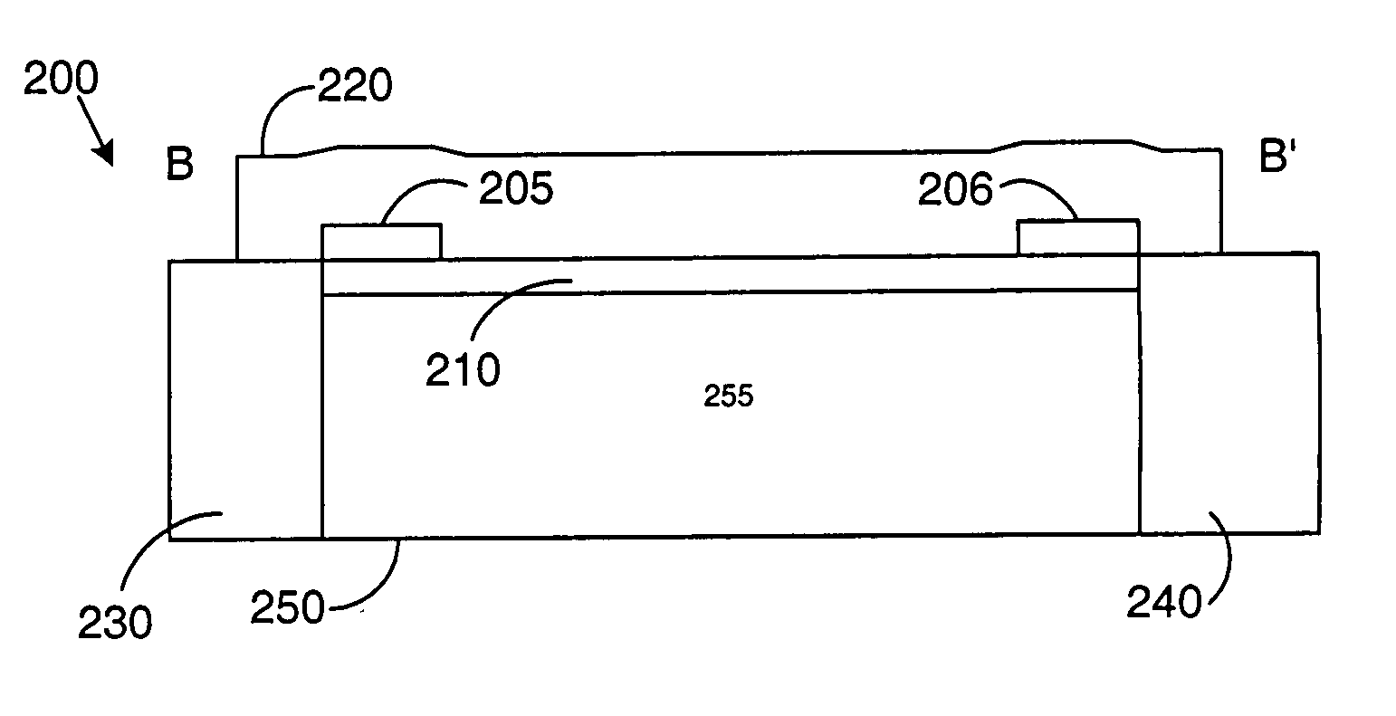
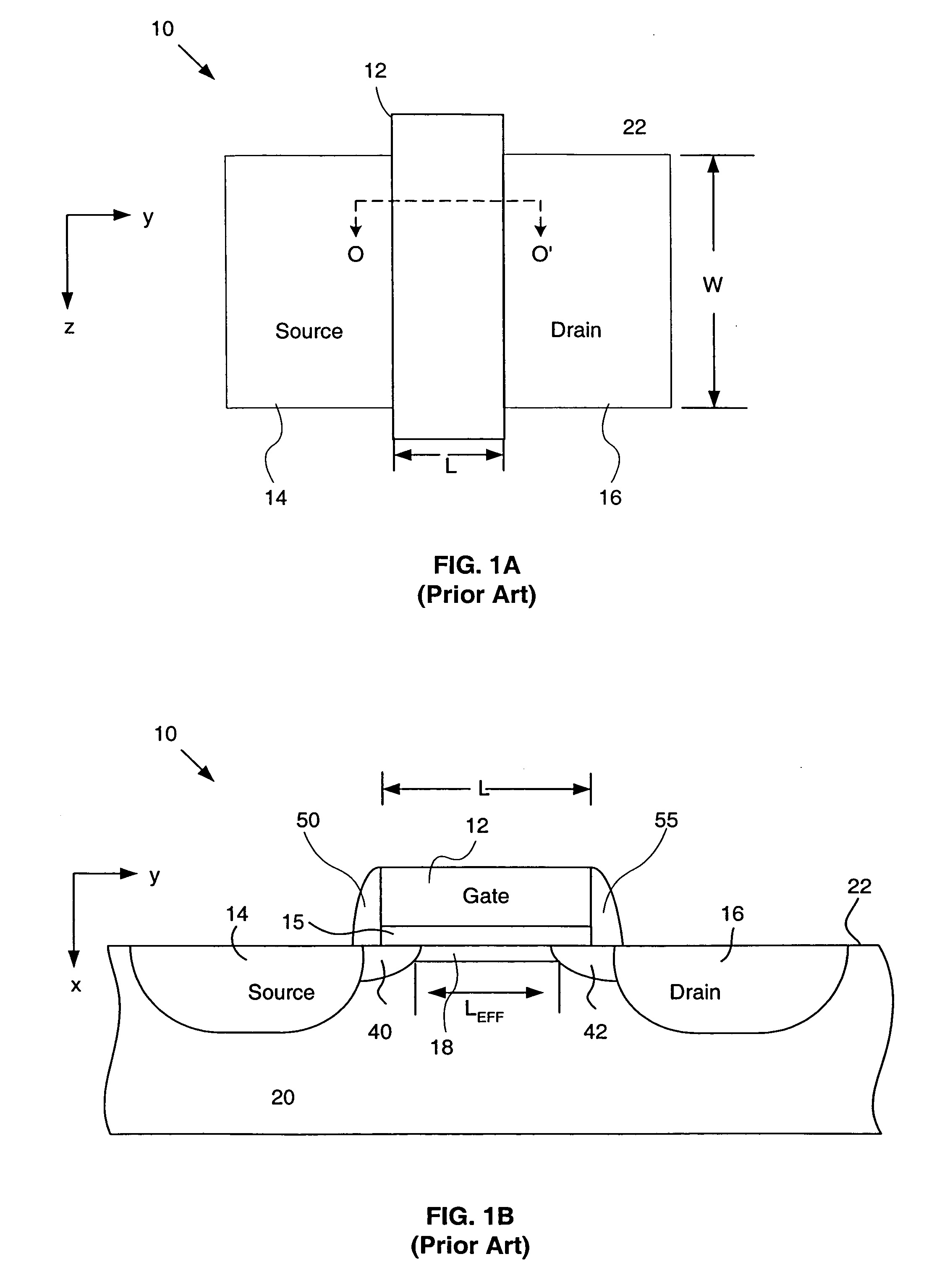
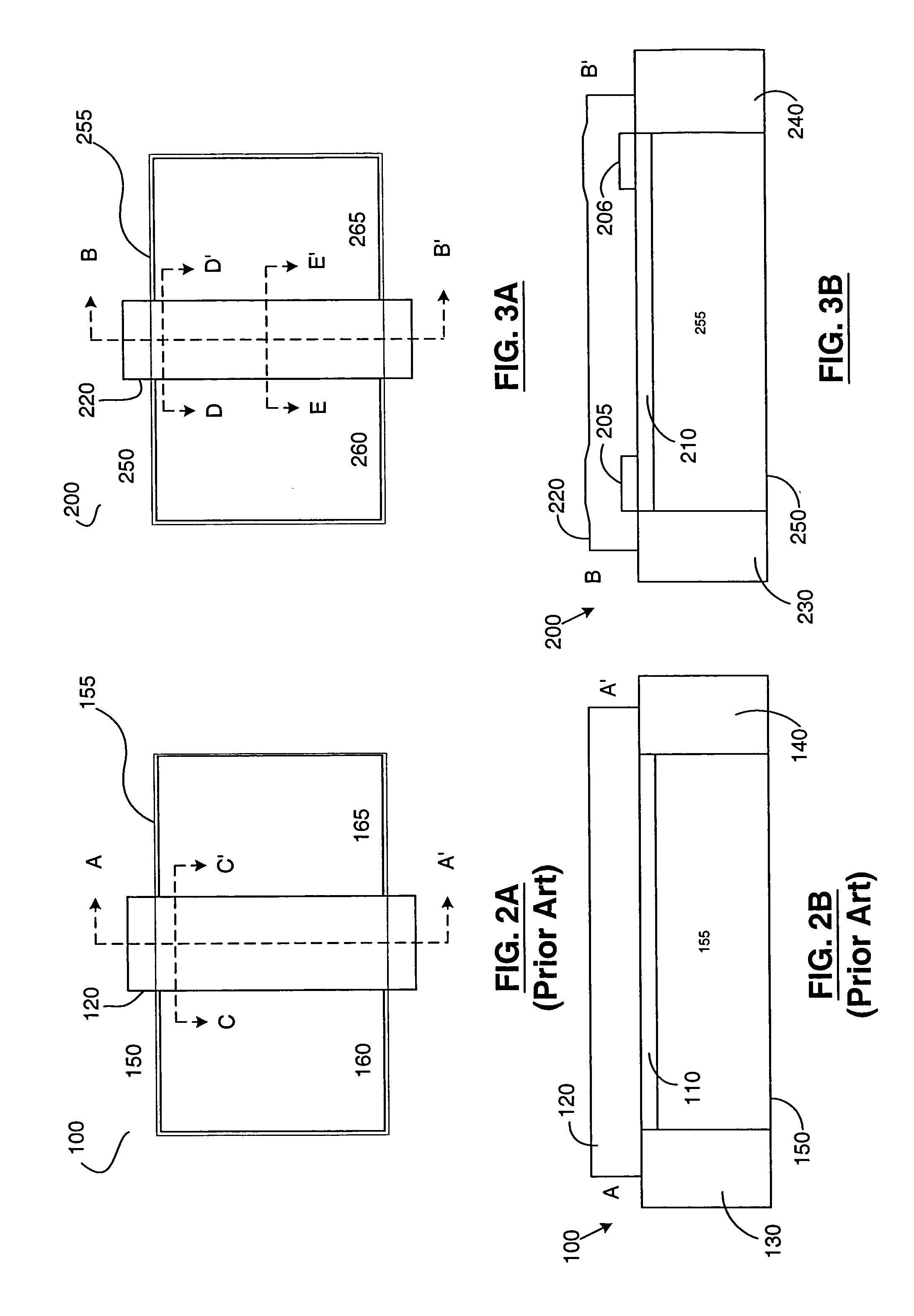
[0024]The figures referred to hereafter are for illustrative purposes and are not to scale or to conform in shape with real devices. FIGS. 2A–D depict a conventional MOSFET device 100. Referring to FIG. 2A, which shows a top view of device 100, device 100 comprises a gate 120 between two diffusion regions, i.e., source 160 and drain 165, in an active region 155 in a semiconductor (such as silicon) substrate 150. Gate 120 is typically formed of polysilicon or metal. Source 160 and drain 165 can be either p-type or n-type diffusion regions in substrate 150.

[0025]FIG. 2B depicts device 100 in vertical cross-section along lines A–A′ in FIG. 2A. As shown in FIG. 2B, gate 120 is on top of a gate oxide layer 110 that is formed on the substrate 150. Regions 130 and 140 represent isolation regions created, for example, by shallow trench isolation (STI) manufacturing techniques.

[0026]FIG. 2C depicts device 100 in vertical cross-section along lines C–C′ in FIG. 2A. As shown in FIG. 2C, device ...


PUM


Abstract

The invention provides a transistor having low leakage currents and methods of fabricating the transistor on a semiconductor substrate. The transistor has a gate and a nonuniform gate oxide under the gate.

Description

CROSS REFERENCE TO RELATED APPLICATIONS[0001]The present application is a divisional and claims priority to application Ser. No. 10 / 189,920, filed Jul. 3, 2002 now U.S. Pat. No. 6,740,944 which claims priority to U.S. Provisional Application Ser. No. 60 / 303,334, filed Jul. 5, 2001.FIELD OF THE INVENTION[0002]The present invention relates to semiconductor devices, and more particularly, to a design of semiconductor devices, such as metal oxide semiconductor field effect transistors (MOSFETs), which have reduced leakage currents, and to a method for fabricating the same.BACKGROUND OF THE INVENTION[0003]FIG. 1A depicts a partial top-view of a conventional MOSFET device 10. As shown in FIG. 1A, MOSFET device has a gate 12 over a substrate 22. A source region 14 and a drain region 16 are located in substrate 22 on opposite sides of gate 12. Gate 12 is referred to as having a length L that extends in the y-direction and a width W that extends in the z-direction, shown in FIG. 1A. Consiste...

Claims


Application Information

Patent Timeline
Patent Type & Authority Patents(United States)
IPC IPC(8): H01L21/28H01L21/02H01L29/40H01L29/423H01L21/336H01L21/8238H01L29/78H01L31/036
CPCH01L21/28123H01L21/823857H01L21/823864H01L29/42368H01L29/6656H01L29/6659H01L29/7833Y10S438/981
Inventor MCELHENY, PETER JOHNLIU, YOWJUANG BILL
Owner ALTERA CORP
Why Eureka
Try Eureka