Non-volatile memory and method with bit line compensation dependent on neighboring operating modes

a non-volatile, operating mode technology, applied in static storage, digital storage, instruments, etc., can solve the problems of unsuitable mobile and handheld environment, bulky disk drives, and easy mechanical failure, and achieve high capacity, non-volatile memory devices. high performance

Active Publication Date: 2005-10-18
SANDISK TECH LLC
View PDF15 Cites 607 Cited by
  • Summary
  • Abstract
  • Description
  • Claims
  • Application Information

AI Technical Summary

Benefits of technology

[0028]These needs for a high capacity and high performance non-volatile memory device are met by having a large page of read / write circuits to read and write a corresponding page of memory cells in parallel. In particular, perturbation effects inherent in high-density chip integration that may introduce errors into reading and programming are either eliminated or minimized.
[0031]In particular, when programming a contiguous page of storage units, every time a storage unit has reached its targeted state and is program-inhibited or locked out from further programming, it creates a perturbation on an adjacent storage unit still under programming. The present invention provides as part of a programming circuit and method in which an offset to the perturbation is added to the adjacent storage unit still under programming. The offset is added by applying a predetermined biased voltage to the bit line of a storage unit still under programming. In particular, if the storage unit is flanked by two neighbors in program inhibit mode, the predetermined offset will compensate for the perturbation from both neighbors. If the storage unit is has only one of its neighbors in program inhibit mode, the bit line offset will be less, sufficient to compensate for just one neighbor. If the storage unit is not flanked by any neighbors in program inhibit mode, the offset will effectively be zero. In this way, an error inherent in programming in parallel high-density memory storage units is eliminated or minimized.

Problems solved by technology

Conventional mass storage, based on rotating magnetic medium such as hard drives and floppy disks, is unsuitable for the mobile and handheld environment.
This is because disk drives tend to be bulky, are prone to mechanical failure and have high latency and high power requirements.
These undesirable attributes make disk-based storage impractical in most mobile and portable applications.
Programming of charge storage memory devices can only result in adding more charge to its charge storage elements.
This approach improves performance but does have a repercussion on the accuracy of read and write operations.
Another issue has to do with bit line to bit line coupling or crosstalk.
This problem becomes more acute with parallel sensing of closely spaced bit lines.
However, the interleaving page architecture is disadvantageous in at least three respects.
First, it requires additional multiplexing circuitry.
Secondly, it is slow in performance.
Thirdly, it is also not optimum in addressing other disturb effects such as field coupling between neighboring charge storage elements at the floating gate level when the two neighbors are programmed at different times, such as separately in odd and even pages.
The problem of neighboring field coupling becomes more pronounced with ever closer spacing between memory transistors.
The conventional architecture of interleaving page exacerbates the error caused by neighboring charge storage unit coupling.
The read errors will become more severe with increasing density, requiring a more accurate read operation and wider partitioning of the threshold window for multi-state implementation.
Performance will suffer and the potential capacity in a multi-state implementation is limited.
This boosted voltage creates a significant perturbation on an adjacent storage unit still under programming.

Method used


Image

  • Non-volatile memory and method with bit line compensation dependent on neighboring operating modes
  • Non-volatile memory and method with bit line compensation dependent on neighboring operating modes
  • Non-volatile memory and method with bit line compensation dependent on neighboring operating modes

Examples


Embodiment Construction

All Bit Line Programming

[0052]The sense module 380 shown in FIG. 4A and FIG. 8 is preferably implemented in a memory architecture configured to perform all-bit-line sensing. In other words, contiguous memory cells in a row are each connectable to a sense module to perform sensing in parallel. Such a memory architecture is also disclosed in co-pending and commonly assigned U.S. patent application Ser. No. 10 / 254,483 filed by Cernea et al., on Sep. 24, 2002 entitled, “Highly Compact Non-Volatile Memory And Method Thereof.” The entire disclosure of said patent application is hereby incorporated herein by reference.

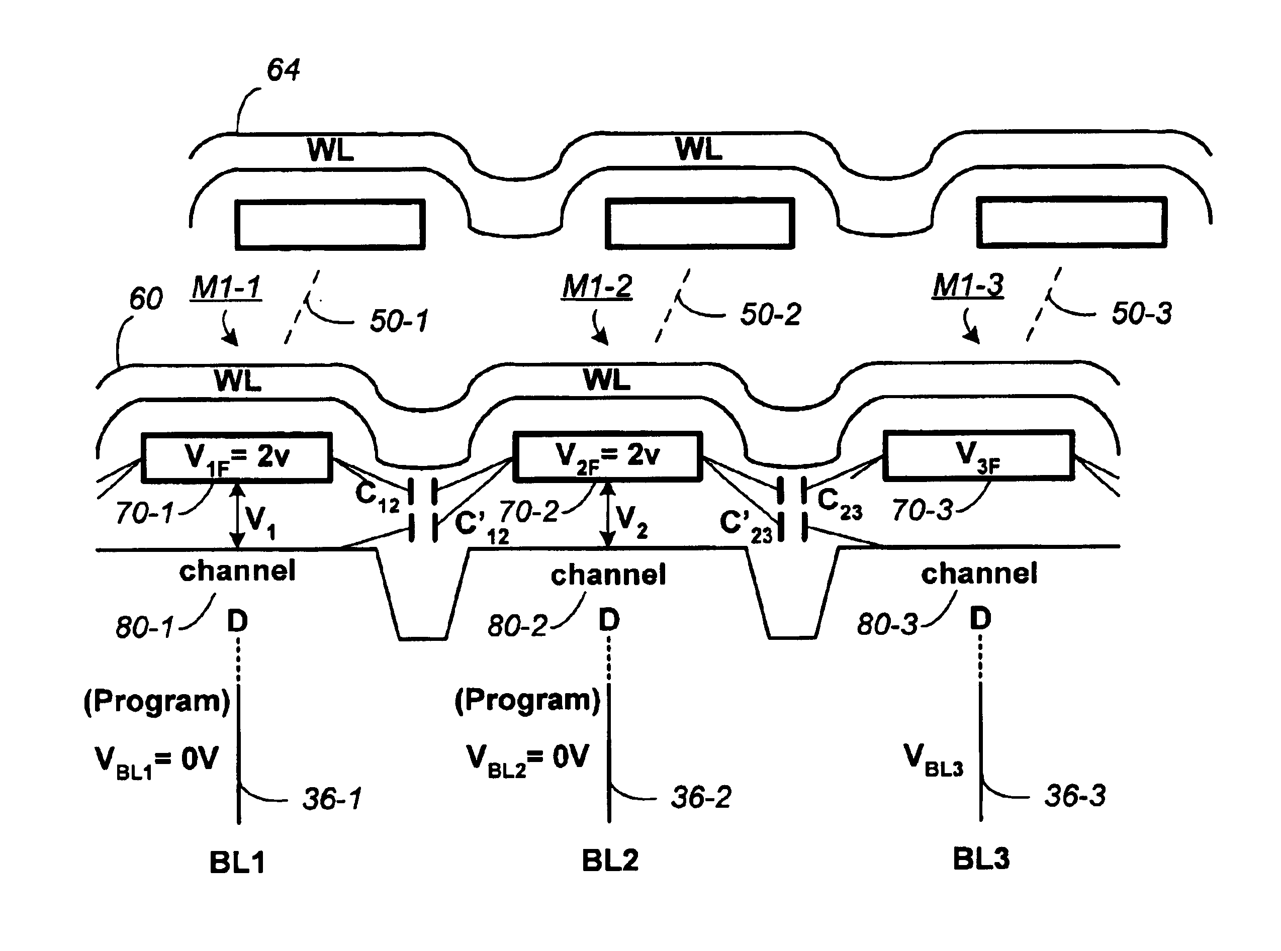
[0053]As described earlier, the number of memory cells in a “page” that are programmed or read simultaneously may vary according to the size of data sent or requested by a host system. Thus, there are several ways to program the memory cells coupled to a single word line, such as (1) programming even bit lines and odd bit lines separately, which may comprise upper page progra...


PUM


Abstract

When programming a contiguous page of memory storage units, every time a memory storage unit has reached its targeted state and is program-inhibited or locked out from further programming, it creates a perturbation on an adjacent memory storage unit still under programming. The present invention provides as part of a programming circuit and method in which an offset to the perturbation is added to the adjacent memory storage unit still under programming. The offset is added as voltage offset to a bit line of a storage unit under programming. The voltage offset is a predetermined function of whether none or one or both of its neighbors are in a mode that creates perturbation, such as in a program inhibit mode. In this way, an error inherent in programming in parallel high-density memory storage units is eliminated or minimized.

Description

FIELD OF THE INVENTION[0001]This invention relates generally to non-volatile semiconductor memory such as electrically erasable programmable read-only memory (EEPROM) and flash EEPROM, and specifically ones having improved programming and sensing circuits for a page of contiguous row of charge storage units.BACKGROUND OF THE INVENTION[0002]Solid-state memory capable of non-volatile storage of charge, particularly in the form of EEPROM and flash EEPROM packaged as a small form factor card, has recently become the storage of choice in a variety of mobile and handheld devices, notably information appliances and consumer electronics products. Unlike RAM (random access memory) that is also solid-state memory, flash memory is non-volatile, retaining its stored data even after power is turned off. In spite of the higher cost, flash memory is increasingly being used in mass storage applications. Conventional mass storage, based on rotating magnetic medium such as hard drives and floppy disk...

Claims


Application Information

Patent Timeline
Patent Type & Authority Patents(United States)
IPC IPC(8): G11C16/06G11C16/34G11C16/04
CPCG11C16/3468G11C16/0483G11C5/063G11C16/08G11C16/12G11C16/24G11C16/26
Inventor KHALID, SHAHZADLI, YANCERNEA, RAUL-ADRIANMOFIDI, MEHRDAD
Owner SANDISK TECH LLC
Why Eureka
Try Eureka