Methods of forming devices, constructions and systems comprising thyristors

a technology of thyristors and forming devices, applied in the field of integrated circuits, can solve the problems of limited performance of tfts, limited carrier mobilities, high power consumption, etc., and achieve the effects of accurate control, fast sram-like performance, and enhanced density of memory cells

Inactive Publication Date: 2005-10-25
MICRON TECH INC
View PDF5 Cites 45 Cited by
  • Summary
  • Abstract
  • Description
  • Claims
  • Application Information

AI Technical Summary

Benefits of technology

[0016]The present invention pertains to SOI constructions comprising at least one memory cell encompassing a transistor and a thyristor. In one aspect, the present invention encompasses a one-device equivalent, gated lateral thyristor-based random access memory (GLTRAM) cell incorporated into a TFT construction. An exemplary memory cell construction includes a crystalline layer comprising silicon and germanium over an electrically insulative material. An access transistor device has an active region extending into the crystalline layer. The entirety of the active region within the crystalline layer is within only a single crystal of the crystalline layer. The transistor device includes a gate, source region and drain region. A thyristor is electrically connected with the source region. The thyristor can be integrated with, and stacked on top of, the access transistor to enhance the density of the memory cell. The geometry of the thyristor can be accurately controlled to provide a lower stored charge volume. Further, the thyristor can be tailored to reduce carrier transit time, which can provide faster performance and improve the gate-assisted turn-off characteristics of the thyristor.
[0017]In various aspects, the lateral thyristor can be fabricated using an MILC technique adopted for TFT technology. Accordingly, the GLTRAM cell can be readily scalable with lithography to provide direct scalability with technology generations. In particular embodiments, the stacked lateral thyristor is integrated by raising the source region of the access transistor using a selective epitaxy process. The stacked configuration of the GLTRAM cell can have a footprint less than 8 F2, and thus can have a higher density than the TRAM cell. Additionally, the GLTRAM cell can have a low standby power consumption during cell operation.

Problems solved by technology

A problem associated with conventional TFT constructions is that grain boundaries and defects can limit carrier mobilities.
High voltage (and therefore high power consumption), and large areas are utilized for the TFTs, and the TFTs exhibit limited performance.
TFTs thus have limited commercial application and currently are utilized primarily for large area electronics.
Performance enhancements of standard field effect transistor devices are becoming limited with progressive lithographic scaling in conventional applications.
Although various techniques have been developed for substantially controlling nucleation and grain growth processes of semiconductor materials, grain orientation control is lacking.
Further, the post-anneal treatment utilized in conjunction with MILC can be unsuitable in applications in which a low thermal budget is desired.
DRAM cells provide good memory density, but are relatively slow.
SRAM cells are faster than DRAM cells, but the area utilized for SRAM cells is large.
The large area associated with six-transistor and four-transistor memory cells has limited the design of high-density SRAM devices.
However, NDR devices tend to suffer from problems such as high standby power consumption, high operating voltages, low speeds and complicated fabrication processes. F. Nemati and J. D. Plummer have disclosed a two-device thyristor-based SRAM cell (TRAM) that includes an access transistor and a gate-assisted, vertical thyristor.
Even so, the geometry and vertical height of the vertical thyristor's p-region limits the turn-off characteristics and the associated cell performance of the gate-assisted, vertical thyristor disclosed by Nemati and Plummer.
The scalability of the TRAM cell and the ability to control the performance of the TRAM cell are also limited.

Method used


Image

  • Methods of forming devices, constructions and systems comprising thyristors
  • Methods of forming devices, constructions and systems comprising thyristors
  • Methods of forming devices, constructions and systems comprising thyristors

Examples


Embodiment Construction

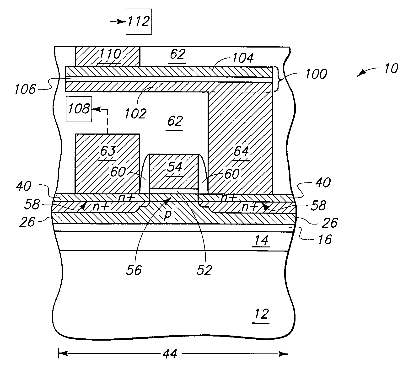
[0038]The present invention pertains to memory devices comprising transistors and thyristors. In particular aspects, the present invention pertains to a one-device equivalent gated lateral thyristor-based SRAM (GLTRAM) cell. The GLTRAM cell includes an access transistor and an integrated, gate-assisted lateral thyristor. The geometry of the lateral thyristor can be accurately controlled to provide a lower stored charged volume. Additional, the geometry of the gate-assisted lateral thyristor is capable of being tailored to reduce carrier transit time, which can provide faster performance and improve gate-assisted turn-off characteristics of the thyristor.

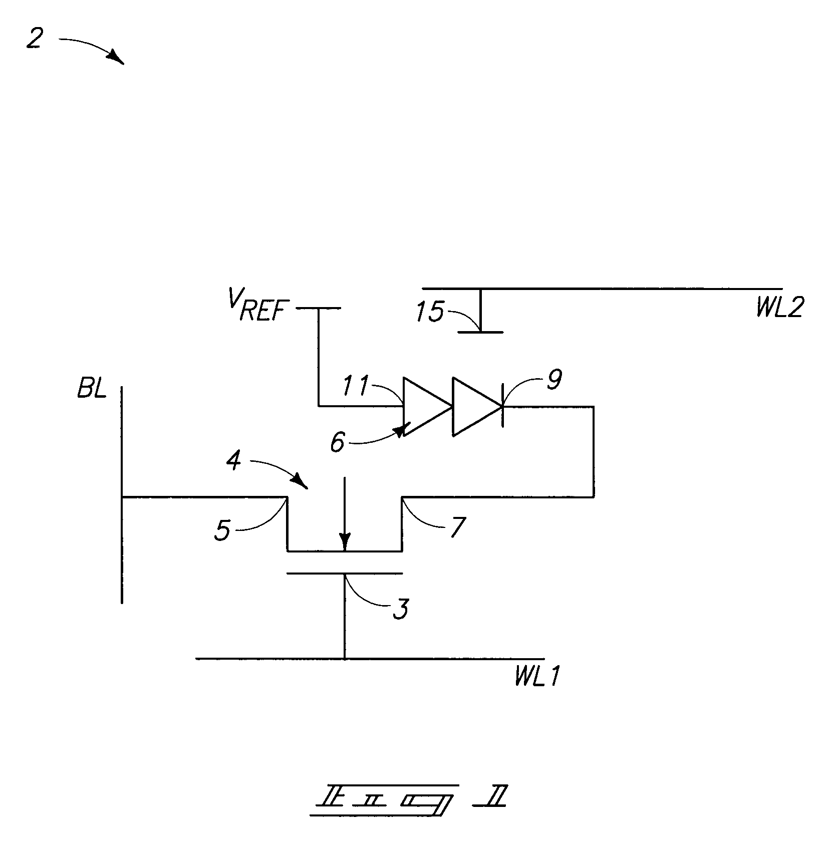
[0039]FIG. 1 illustrates a circuit schematic of an exemplary GLTRAM cell 2. Cell 2 includes an access transistor 4 and a thyristor 6. Access transistor 4 can be, for example, an NFET transistor. Thyristor 6 is illustrated as a p+ / n / p / n+ thyristor (specifically, it is illustrated as two diodes in the shown schematic diagram). One defi...


PUM


Abstract

The invention includes SOI constructions containing one or more memory cells which include a transistor and a thyristor. In one aspect, a scalable GLTRAM cell provides DRAM-like density and SRAM-like performance. The memory cell includes an access transistor and a gated-lateral thyristor integrally formed above the access transistor. The cathode region (n+) of the stacked lateral thyristor device (p+ / n / p / n+) is physically and electrically connected to one of the source / drain regions of the FET to act as the storage node for the memory cell. The FET transistor can include an active region which extends into a Si / Ge material. The material comprising Si / Ge can have a relaxed crystalline lattice, and a layer having a strained crystalline lattice can be between the material having the relaxed crystalline lattice and the transistor gate. The device construction can be formed over a versatile substrate base.

Description

RELATED PATENT DATA[0001]This patent resulted from a continuation application of U.S. patent application Ser. No. 10 / 364,213, which was filed Feb. 10, 2003.TECHNICAL FIELD[0002]This disclosure relates generally to integrated circuits, and more particularly, to memory cells containing thyristors. Exemplary memory cells comprise gated lateral thyristor-containing random access memory (GLTRAM) cells incorporated into TFT constructions. Such constructions can be formed over a versatile substrate base.BACKGROUND OF THE INVENTION[0003]SOI technology differs from traditional bulk semiconductor technologies in that the active semiconductor material of SOI technologies is typically much thinner than that utilized in bulk technologies. The active semiconductor material of SOI technologies will typically be formed as a thin film over an insulating material (typically oxide), with exemplary thicknesses of the semiconductor film being less than or equal to 2000 Å. In contrast, bulk semiconductor...

Claims


Application Information

Patent Timeline
Patent Type & Authority Patents(United States)
IPC IPC(8): H01L21/336H01L29/786H01L21/70H01L29/66H01L21/02H01L21/84H01L21/8244H01L27/06H01L27/108H01L27/11H01L27/12H01L31/072
CPCH01L21/84H01L27/0688H01L27/1203H01L29/66742H01L29/7842H01L29/78684H01L29/78687H01L27/10808H01L27/11H10B12/31H10B10/00
Inventor BHATTACHARYYA, ARUP
Owner MICRON TECH INC
Why Eureka
Try Eureka