
Off chip driver

a driver circuit and chip technology, applied in logic circuits, pulse techniques, reliability increasing modifications, etc., can solve the problems of unwanted signal reflection, voltage overshoot, voltage undershoot and timing problems, additional circuitry of the plurality of elements adds unwanted capacitance to the output impedance, etc., to achieve high-quality control of output impedance, rapid switching, and no noise and ringing.

Inactive Publication Date: 2005-10-25
POLARIS INNOVATIONS LTD
View PDF7 Cites 6 Cited by
  • Summary
  • Abstract
  • Description
  • Claims
  • Application Information

AI Technical Summary

Benefits of technology

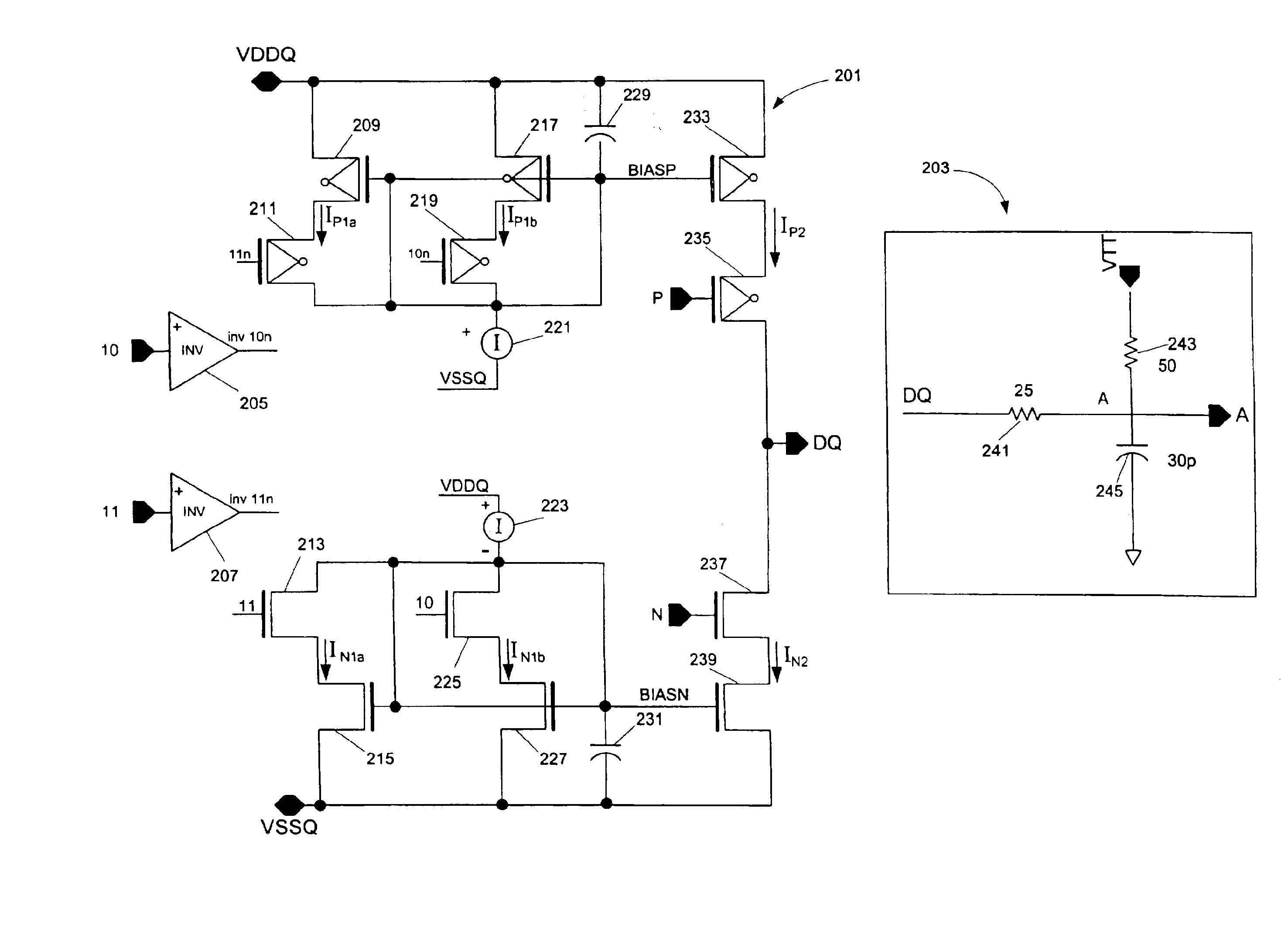
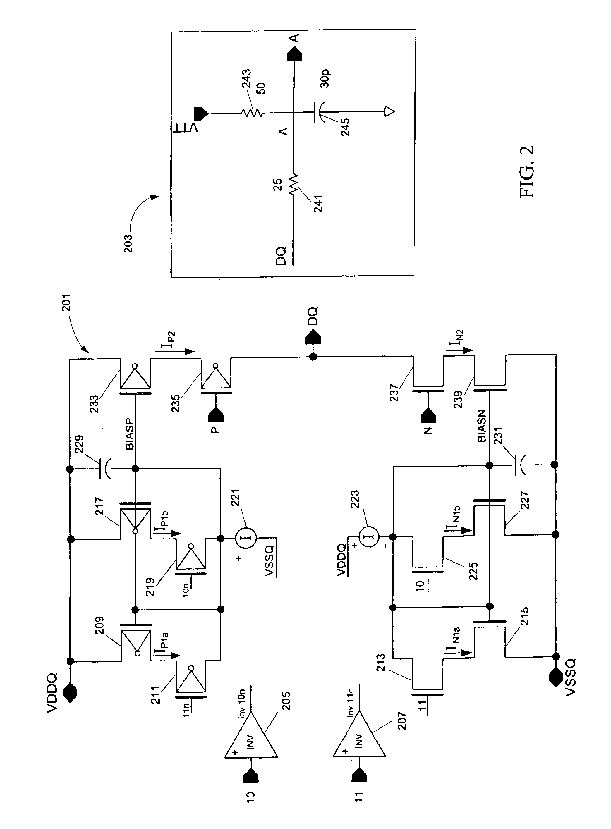
[0006]The present invention provides an off chip driver circuit that avoids these problems and provides highly accurate control of output impedance and rapid switching between the high and low logical levels without the generation of noise and ringing. This performance is achieved by coupling to both the pull up transistor and the pull down transistor an additional transistor that acts as a current mirror transistor and by controlling the slew rate (rate of change of output voltage) of the gate signals driving the pull up and pull down transistors. The pull up transistor's current mirroring transistor controls the driver's drive current (and output impedance) during the high logical level, and the pull down transistor's current mirroring transistor controls the driver's drive current (and output impedance) during the low logical level. By controlling the current that the current mirroring transistors mirror, the driver's drive current (and output impedance) also is controlled. By controlling the slew rate of the gate signals driving the pull up and pull down transistors, noise and ringing during switching between the high and low logical levels are substantially diminished.

Problems solved by technology

A failure to match the driver's output impedance to the input impedance of the load can cause unwanted signal reflections, voltage overshoots, voltage undershoots and timing problems.
A problem with these prior art systems is that the additional circuitry of the plurality of elements adds unwanted capacitance to the output impedance.
This oversizing undesirably increases the DC output impedance of the driver.
Also, the rapid switching generates noise on the output signal and ringing on the power buses.

Method used


Image

  • Off chip driver
  • Off chip driver
  • Off chip driver

Examples


Embodiment Construction

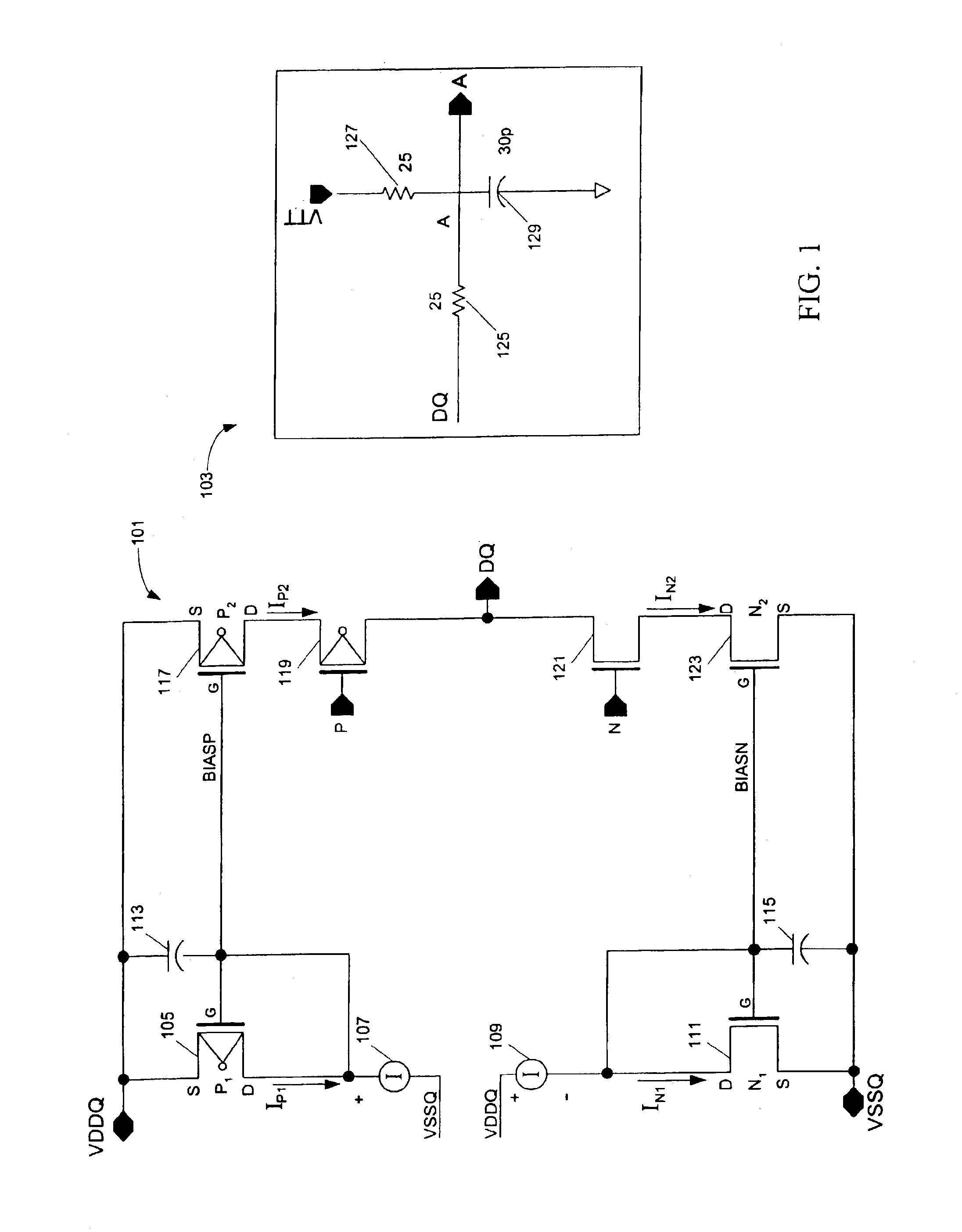
[0019]An off chip driver 101 in accordance with the present invention is shown in FIG. 1. The output signal on terminal DQ of driver 101 drives off chip load 103. Load 103 is a Stub Series Terminated Logic (“SSTL2”), Class 2 load with a 25 ohm series resistor 125, a 25 ohm termination resistor 127 to VTT and a 30 picofarad capacitor 129 to ground.

[0020]Off chip driver 101 includes current sources 107 and 109, pull up transistor 119, pull down transistor 121 and current mirror transistors 105, 117, 111 and 123. These elements are connected as shown in FIG. 1. Pull up transistor 119 is a P-channel CMOS transistor, and pull down transistor 121 is an N-channel CMOS transistor. Current mirror transistors 105 and 117 are P-channel CMOS transistors (also labeled P1 and P2, respectively, in FIG. 1), and current mirror transistors 111 and 123 are N-channel CMOS transistors (also labeled N1 and N2, respectively, in FIG. 1). Capacitors 113 and 115 provide voltage stability between the gates an...


PUM


Abstract

A system and method is provided for controlling the impedance and current of an off chip driver circuit to match to load driven by the driver and for reducing noise and ringing in the off chip driver circuit. The driver comprises a pull up transistor for switching the output of the driver to a high-voltage, a pull down transistor for switching the output of the driver to a low voltage, a first current mirror transistor coupled to the pull up transistor for controlling the current transmitted to a load connected to the driver when the output of the driver is at the high-voltage, and a second current mirror transistor coupled to the pull down transistor for controlling the current transmitted to the load when the output of the driver is at the low voltage. In addition, the driver may include a first pre-driver providing a gate signal for the pull up transistor having a controlled slew rate and a second pre-driver providing a gate signal for the pull down transistor having a controlled slew rate.

Description

FIELD OF THE INVENTION[0001]The present invention relates to an off chip driver circuit and, in particular, to a system and method for controlling the impedance and current of an off chip driver circuit to match the load driven by the driver. The present invention further relates to a system and method for reducing noise and ringing in an off chip driver circuit.BACKGROUND OF THE INVENTION[0002]Semiconductor chips, such as semiconductor memory chips and semiconductor processor chips, generate logical high signals and logical low signals that eventually must be transmitted to one or more devices (“the load”) located off of the chip. In order to transmit these output signals to the load, the chip includes an off chip driver circuit that receives the chip's output signals and transmits these signals to the load. The driver circuit generally is fabricated using P-channel and N-channel field effect transistors (FETs) and, in particular, metal oxide semiconductor (MOS) or complementary me...

Claims


Application Information

Patent Timeline
Patent Type & Authority Patents(United States)
IPC IPC(8): H03K19/003H03K19/0185H03K17/16H03K19/017H03K19/01
CPCH03K17/163H03K19/00384H03K19/01707H03K19/018585
Inventor TERLETZKI, HARTMUDFRANKOWSKY, GERD H.LEHMANN, GUNTHER R.
Owner POLARIS INNOVATIONS LTD
Learn More