Magnetic element utilizing spin-transfer and half-metals and an MRAM device using the magnetic element

a magnetic element and spin-transfer technology, applied in the field of magnetic memory systems, can solve the problems of increasing cross talk and power consumption, increasing physical area and complexity, and obstacles at higher memory cell densities, so as to reduce high switching current, low power consumption, and high density

Inactive Publication Date: 2005-10-25
SAMSUNG SEMICON
View PDF9 Cites 297 Cited by
  • Summary
  • Abstract
  • Description
  • Claims
  • Application Information

AI Technical Summary

Benefits of technology

[0030]The present invention provides a way to reduce the high switching current exhibited by a conventional spin-transfer stack. The present invention also provides a magnetic memory element that can be used in a memory array having high dens...

Problems solved by technology

Although conventional magnetic memory 200 using conventional spin tunneling junctions 100′ can function, there are obstacles at higher memory cell densities.
This relatively large current can cause a host of problems in a conventional magnetic memory array 200.
For example, cross talk and power consumption increases accordingly.
Additionally, the driving circuits required for driving the current that generates the switching field at a selected memory cell 220 also increase in physical area and complexity.
The upper limit on the magnitude of the write current can lead to reliability issues because cells that are relatively harder to switch than others based on fabrication and material non-uniformity will fail to write consistently.
The high current density that is required for inducing the spin-transfer effect, however, could destroy the thin insulating barrier due to ohmic dissipation.
Thus, an MRAM having conventional spin tunneling junction magnetic elements 100′ that have a high Ra value may not be able to be used with the spin-transfer effect for writing to the magnetic memory cells.
The single-spacer spin-transfer stack type suffers numerous disadvantages, including an extremely small signal, a low resistance, and a high sw...

Method used


Image

  • Magnetic element utilizing spin-transfer and half-metals and an MRAM device using the magnetic element
  • Magnetic element utilizing spin-transfer and half-metals and an MRAM device using the magnetic element
  • Magnetic element utilizing spin-transfer and half-metals and an MRAM device using the magnetic element

Examples


Embodiment Construction

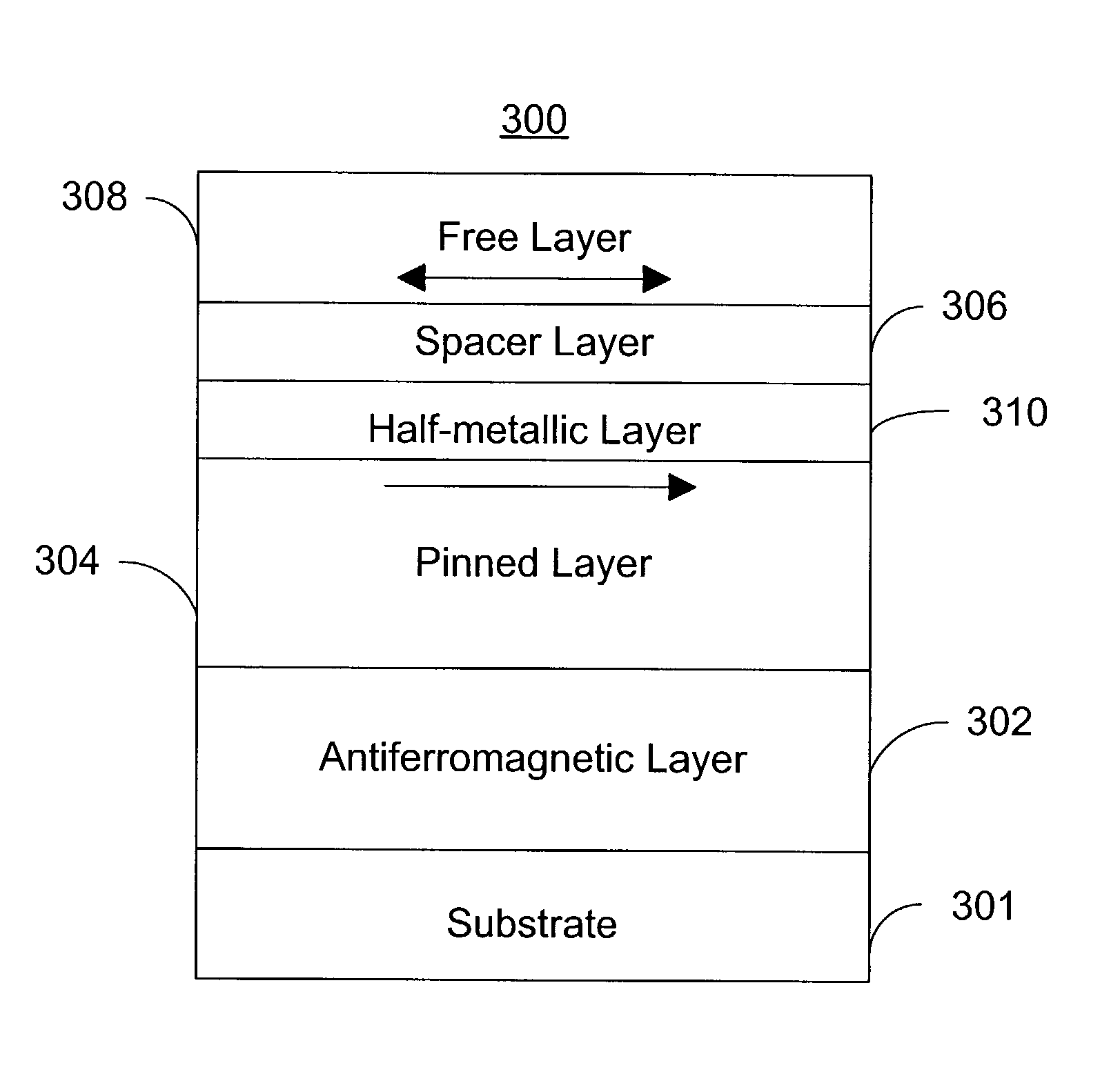
[0051]The present invention provides a spin-transfer stack device that has a reduced switching current and that can be used in a memory array having high density. Further, a spin-transfer stack device of the present invention provides low power consumption, low cross talk, and has high reliability, while providing a useable read signal. To achieve these and other advantages, the present invention provides different types of spin-transfer stack devices that replace magnetic layers with layers of a half-metallic material and / or use a continuous or a discontinuous layer of a half-metallic material on the magnetic layers.

[0052]One exemplary embodiment of the present invention provides a single-spacer spin-transfer stack device that uses thin coating of a half-metallic material that is approximately 100 Å thick or less that is deposited on top of the pinned layer, thereby reducing the effects of the undesirable material characteristics and still keep the high polarization.

[0053]FIGS. 3A ...


PUM


Abstract

A magnetic element that can be used in a memory array having high density includes a pinned layer, a half-metallic material layer, a spacer (or a barrier) layer and a free layer. The half-metallic material layer is formed on the pinned layer and preferably has a thickness that is less than about 100 Å. The half-metallic material layer can be formed to be a continuous layer or a discontinuous on the pinned layer. The spacer (or barrier) layer is formed on the half-metallic material layer, such that the spacer (or barrier) layer is nonmagnetic and conductive (or insulating). The free layer is formed on the spacer (or barrier) layer and has a second magnetization that changes direction based on the spin-transfer effect when a write current passes through the magnetic element.

Description

BACKGROUND OF THE INVENTION[0001]1. Field of the Invention[0002]The invention relates to magnetic memory systems. More particularly, the present invention relates to a method and system for providing an element that employs a spin-transfer effect in switching and that can be used in a magnetic memory, such as a magnetic random access memory (“MRAM”).[0003]2. Description of the Related Art[0004]Magnetic memories are used for storing data. One type of memory element of interest utilizes magnetoresistance properties of a magnetic element for storing data. FIGS. 1A and 1B respectively depict cross sectional views of a conventional spin valve magnetic element 100 and a conventional spin tunneling junction magnetic element 100′. As shown in FIG. 1A, conventional spin valve magnetic element 100 includes a conventional antiferromagnetic (AFM) layer 102, a conventional pinned layer 104, a conventional spacer layer 106, and a conventional free layer 108. Conventional pinned layer 104 and conv...

Claims


Application Information

Patent Timeline
IPC IPC(8): G11C11/00G11C11/16
CPCG11C11/16H01L43/08H10N50/10
Inventor NGUYEN, PAUL P.HUAI, YIMING
Owner SAMSUNG SEMICON
Why Eureka
Try Eureka