Semiconductor device and manufacturing method thereof

a semiconductor device and manufacturing method technology, applied in the direction of semiconductor devices, semiconductor/solid-state device details, electrical apparatus, etc., can solve the problems of deteriorating defect in the connecting part between the interposers, and affecting the mechanical reliability of the package, so as to reduce the distance between the first and second interposers, improve the mechanical strength of the connection between the interposers, and reduce the overall thickness of the semiconductor device

Inactive Publication Date: 2005-11-01
FUJITSU LTD
View PDF8 Cites 38 Cited by
  • Summary
  • Abstract
  • Description
  • Claims
  • Application Information

AI Technical Summary

Benefits of technology

[0018]According to the above-mentioned invention, there is no need to encapsulate the second semiconductor element provided between the first and second interposers. Thus, a distance between the first and second interposers can be reduced, which results in a reduction in an overall thickness of the semiconductor device. Additionally, since the second semiconductor element and the first interposer are bonded to each other by the adhesive, a mechanical strength of the connection between the interposers is improved, which prevents warp of the interposers. Further, since the second semiconductor element is bonded to the first interposer by the adhesive, a heat generated in the first semiconductor element can be effi

Problems solved by technology

Additionally, since the interposers are connected and fixed to each other by the solder balls provided in the peripheral portion of the interposers, if a warp occurs in the interposers in a stacking process of an assembling process of the semiconductor package, a defect may occur in the connecting part between the interposers.
Moreover, when mounting the complete semiconductor package onto a substrate, a def

Method used


Image

  • Semiconductor device and manufacturing method thereof
  • Semiconductor device and manufacturing method thereof
  • Semiconductor device and manufacturing method thereof

Examples


second embodiment

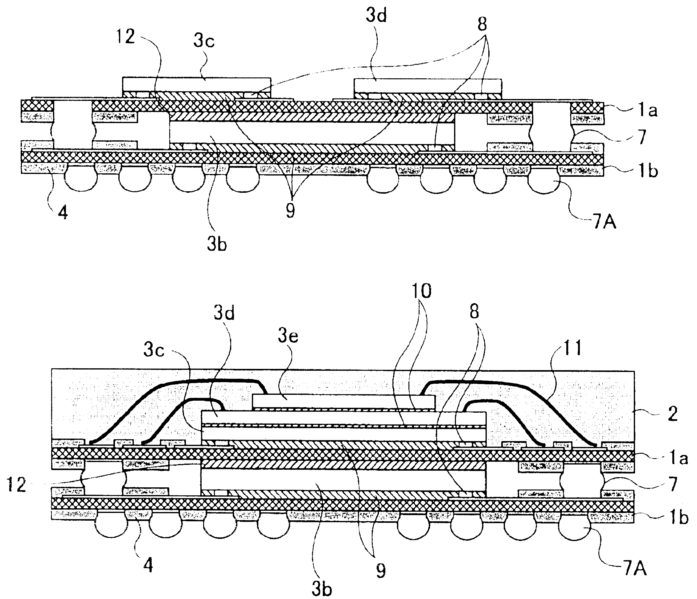
[0056]The semiconductor device according to the present invention is configured by mounting a plurality of semiconductor chips 3c, 3d and 3e onto the top surface of the interposer shown in FIG. 2 in a stacked state.

[0057]The semiconductor chip 3c is electrically connected to the top surface of the interposer 1a through bumps 8. The semiconductor chip 3c and the interposer 1a are bonded by the under-fill adhesive 9.

[0058]The semiconductor chip 3d is mounted on the back surface of the semiconductor chip 3c in a stacked state, and is bonded to the semiconductor chip 3c by a die-bonding adhesive 10. As for the die-bonding adhesive 10, a resin material such as epoxy, acrylics or polyimide can be used. The semiconductor chip 3d is mounted on the semiconductor chip 3c with the circuit forming surface up, and is electrically connected to the electrode pads formed on the top surface of the interposer 1a by Au wires.

[0059]The semiconductor chip 3e is smaller than the semiconductor chip 3d, an...

first embodiment

[0061]The semiconductor device according to the present embodiment can provide the same effects as the semiconductor device according to the above-mentioned Additionally, a heat from the semiconductor chips 3c, 3d and 3e, which are stacked on the top surface of the interposer 1a, is also transmitted to the lower interposer 1b through the semiconductor chip 3a and the semiconductor chip 3b bonded to the semiconductor chip 3a. Thereby, the heat from the semiconductor chips 3c, 3d and 3e, which are stacked on the top surface of the interposer 1a, can also be efficiently emitted outside through the lower interposer 1b.

[0062]It should be noted that, although three semiconductor chips are stacked on the interposer 1a and encapsulated by a seal resin, the present invention is not limited to the number of semiconductor chips and the method of mounting, and a different number of semiconductor chips may be mounted by a different mounting method.

[0063]Next, a description will be given, with ...

third embodiment

[0064]The semiconductor device according to the present invention has a structure in which the semiconductor chip 3c is mounted on the top surface of the interposer 1a of the semiconductor device shown in FIG. 2. The semiconductor chip 3c is electrically connected to the top surface of the interposer 1a through bumps 8. The semiconductor chip 3c and the interposer 1a are bonded by the under-fill adhesive 9.

[0065]Since the semiconductor chip 3c stacked on the interposer 1a is mounted with the circuit forming surface down and the under-fill adhesive 9 is filled between the circuit forming surface and the interposer 1a, there is no need to encapsulate the semiconductor chip 3c by a seal resin.

[0066]As mentioned above, the semiconductor chip 3b is electrically connected to the top surface of the interposer 1b through the bumps 8. Moreover, the interposers 1a and 1b are electrically connected by the solder balls 7, and the solder balls 7A as external connection terminals are provided on ...


PUM


Abstract

A stacked-type semiconductor device has a reduced overall height and an improved reliability in the mechanical strength of the stacked structure. The semiconductor device also has an improved heat release characteristic. A first interposer has a surface on which first electrode pads are formed and a first semiconductor element is mounted with a circuit forming surface facing the first interposer. A second interposer has a surface on which second electrode pads are formed and a second semiconductor element is mounted with a circuit forming surface facing the second interposer. External connection terminals are provided on a surface of the second interposer opposite to the surface on which the second semiconductor element is mounted. The first and second interposers are electrically connected to each other by conductive members provided therebetween. A back surface of the first semiconductor element and a back surface of the second semiconductor element are fixed to each other by an adhesive.

Description

[0001]This application is a divisional of application Ser. No. 10 / 272,013, filed Oct. 17, 2002, now U.S. Pat. No. 6,781,241.BACKGROUND OF THE INVENTION[0002]1. Field of the Invention[0003]The present invention generally relates to semiconductor devices and, more particularly, to a semiconductor device having a three-dimensional structure in which a plurality of semiconductor devices and semiconductor elements are stacked, and a manufacturing method of such a semiconductor device.[0004]With the development of electric equipments in recent years, a demand for miniaturization in dimensions and thickness, multi-function, high-performance and high-density in the semiconductor devices has been increasing. In order to cope with such a demand, the structure of the semiconductor devices has been shifting to a three-dimensional structure in which a plurality of semiconductor devices or a plurality of semiconductor elements are stacked.[0005]2. Description of the Related Art[0006]Japanese Laid...

Claims


Application Information

Patent Timeline
IPC IPC(8): H01L25/065H01L25/18H01L25/07H01L25/10H01L25/11
CPCH01L25/03H01L25/0657H01L25/105H01L2224/16H01L2224/32145H01L2224/32225H01L2224/48091H01L2224/48227H01L2224/73204H01L2224/73253H01L2224/73265H01L2225/0651H01L2225/06513H01L2225/06517H01L2225/0652H01L2225/06541H01L2225/06558H01L2225/06572H01L2924/01079H01L2924/15311H01L2924/15331H01L2924/00014H01L2224/45144H01L2924/3511H01L2224/16225H01L2924/00012H01L2924/00011H01L2225/1023H01L2225/1058H01L2225/1094H01L2924/00H01L24/73H01L23/48
Inventor NISHIMURA, TAKAOUNO, TADASHIONODERA, HIROSHITAKASHIMA, AKIRA
Owner FUJITSU LTD
Why Eureka
Try Eureka