SiOCH low k surface protection layer formation by CxHy gas plasma treatment

Inactive Publication Date: 2005-11-08
TAIWAN SEMICON MFG CO LTD
View PDF14 Cites 74 Cited by
  • Summary
  • Abstract
  • Description
  • Claims
  • Application Information

AI Technical Summary

Benefits of technology

[0017]Conventional damascene processing follows as described for the first embodiment. This method also prevents an oxide recess from occurring

Problems solved by technology

One problem associated with the damascene process is that etch stop layer 13 which is typically a low k material like silicon carbide or PbO does not have good adhesion to the ARL in the patterning step or to metal barrier layer 15.
As a result, various types of defects occur that degrade device performance.
This can lead to defects such as scratches in etch stop 13 or even in dielectric layer 12.
If the defects are detected before further process

Method used


Image

  • SiOCH low k surface protection layer formation by CxHy gas plasma treatment
  • SiOCH low k surface protection layer formation by CxHy gas plasma treatment
  • SiOCH low k surface protection layer formation by CxHy gas plasma treatment

Examples


first embodiment

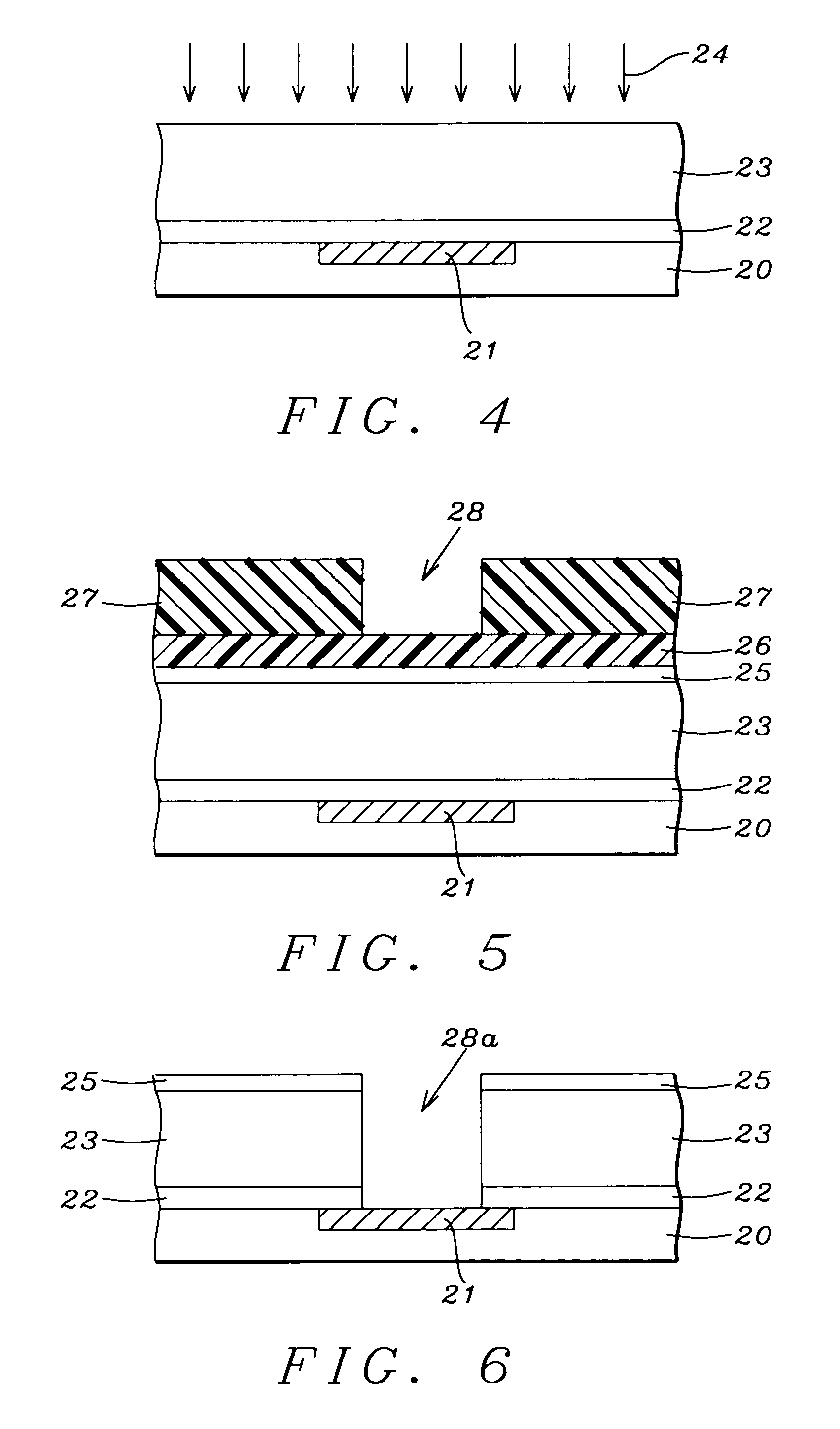
[0022]A first embodiment is set forth in FIGS. 4 to 8. These figures are not necessarily drawn to scale and are presented as examples and not as limitations of the scope of the present invention. Referring to FIG. 4, a substrate 20 is provided that is typically silicon and which generally contains one or more conductive layers such as layer 21 and insulating layers (not shown). The conductive layer may be separated from an adjoining insulating layer by a barrier metal layer (not shown) that forms a liner in a hole or trench to protect the conductive layer from trace amounts of moisture or chemical residues in the insulating material. A method such as a CMP step is used to planarize conductive layer 21 so that it is coplanar with the surface of substrate 20.

[0023]An etch stop layer 22 comprised of a material such as silicon nitride, silicon oxynitride, or silicon carbide is deposited by a CVD or PECVD technique on substrate 20 and conductive layer 21. Etch stop layer 22 protects cond...

second embodiment

[0032]A second embodiment is illustrated in FIGS. 9 to 13 in which a plasma treatment to modify a low k dielectric layer is comprised of two gases that can act together or separately. Referring to FIG. 9, a substrate 40 is provided that is typically silicon and which generally contains one or more conductive layers such as layer 41 and insulating layers (not shown). The conductive layer may be separated from an adjoining insulating layer by a barrier metal layer (not shown) that forms a liner in a hole or trench to protect the conductive layer from trace amounts of moisture or chemical residues in the insulating material. A CMP step is used to planarize conductive layer 41 so that it is coplanar with the surface of substrate 40.

[0033]An etch stop layer 42 comprised of a material such as silicon nitride, silicon oxynitride, or silicon carbide is deposited by a CVD or PECVD technique on substrate 40 and conductive layer 41. Etch stop layer 42 protects conductive layer 41 from aqueous ...


PUM


Abstract

A method of protecting a low k dielectric layer that is preferably comprised of a material containing Si, O, C, and H is described. The dielectric layer is subjected to a gas plasma that is generated from a CXHY gas which is preferably ethylene. Optionally, hydrogen may be added to the CXHY gas. Another alternative is a two step plasma process involving a first plasma treatment of CXHY or CXHY combined with H2 and a second plasma treatment with H2. The modified dielectric layer provides improved adhesion to anti-reflective layers and to a barrier metal layer in a damascene process. The modified dielectric layer also has a low CMP rate that prevents scratch defects and an oxide recess from occurring next to the metal layer on the surface of the damascene stack. The plasma treatments are preferably done in the same chamber in which the dielectric layer is deposited.

Description

FIELD OF THE INVENTION[0001]The invention relates to the field of fabricating integrated circuits and other electronic devices and in particular to a method of protecting a low k dielectric layer to improve adhesion to adjacent layers and to reduce defects during a subsequent chemical mechanical polish step.BACKGROUND OF THE INVENTION[0002]An important process during the fabrication of integrated circuits for semiconductor devices is formation of metal interconnects that provide electrical paths between conductive layers. Metal interconnects consist of trenches that provide horizontal connections between conductive features and via or contact holes that provide vertical connections between metal layers. These metal lines are separated by insulating or dielectric materials to prevent capacitance coupling or crosstalk between the metal wiring. Recent improvements in dielectric layers have involved replacing SiO2 that has a dielectric constant (k) of about 4 with a low k material such ...

Claims


Application Information

Patent Timeline
IPC IPC(8): H01L21/4763H01L21/02H01L21/768
CPCH01L21/3105H01L21/31144H01L21/3212H01L21/76802H01L21/76826H01L21/76829H01L21/76835
Inventor BAO, TIEN-ILU, HSIN-HSIENLI, LIH-PINGKO, CHUNG-CHISONG, AARONJANG, SYUN-MING
Owner TAIWAN SEMICON MFG CO LTD
Why Eureka
Try Eureka