Method for fabricating nanoscale patterns in light curable compositions using an electric field

a technology of light curable compositions and nanoscale patterns, which is applied in the direction of electric/magnetic/electromagnetic heating, instruments, photomechanical equipment, etc., can solve the problems of prohibitively expensive equipment and processes, the resolution of methods reaching their limits, and the difficulty of obtaining a light source with sufficient output intensity at these wavelengths of light, etc., to achieve the effect of improving the aspect ratio of structures

Inactive Publication Date: 2005-11-15
THE UNIV OF TEXAS SYST
View PDF251 Cites 88 Cited by
  • Summary
  • Abstract
  • Description
  • Claims
  • Application Information

AI Technical Summary

Benefits of technology

[0011]After the polymerizable composition is cured, the structures may be further defined by etching the cured polymerizable composition. Etc

Problems solved by technology

However, these methods are reaching their limits in resolution.
At these short wavelengths, few, if any, materials are optically transparent and therefore imaging systems typically have to be constructed using complicated reflective optics [1].
Furthermore, obtaining a light source that has sufficient output intensity at these wavelengths of light is difficult.
Such systems lead to extremely complicated equipment and processes that appear to be prohibitively expensive.
High-

Method used


Image

  • Method for fabricating nanoscale patterns in light curable compositions using an electric field
  • Method for fabricating nanoscale patterns in light curable compositions using an electric field
  • Method for fabricating nanoscale patterns in light curable compositions using an electric field

Examples


Embodiment Construction

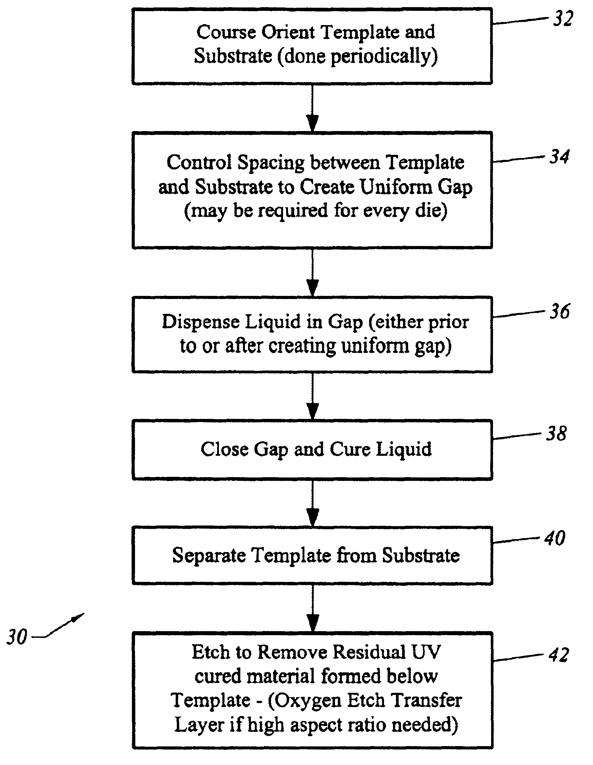
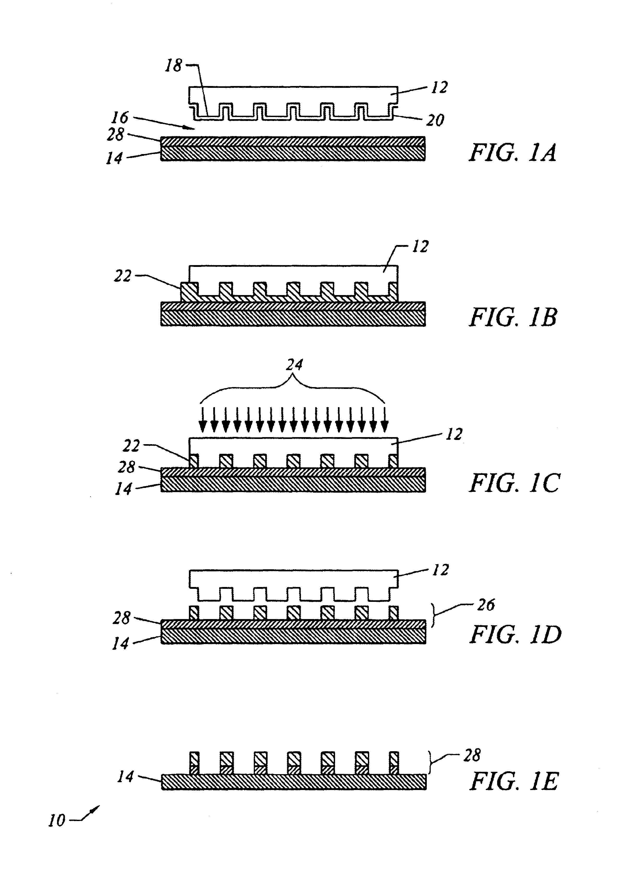
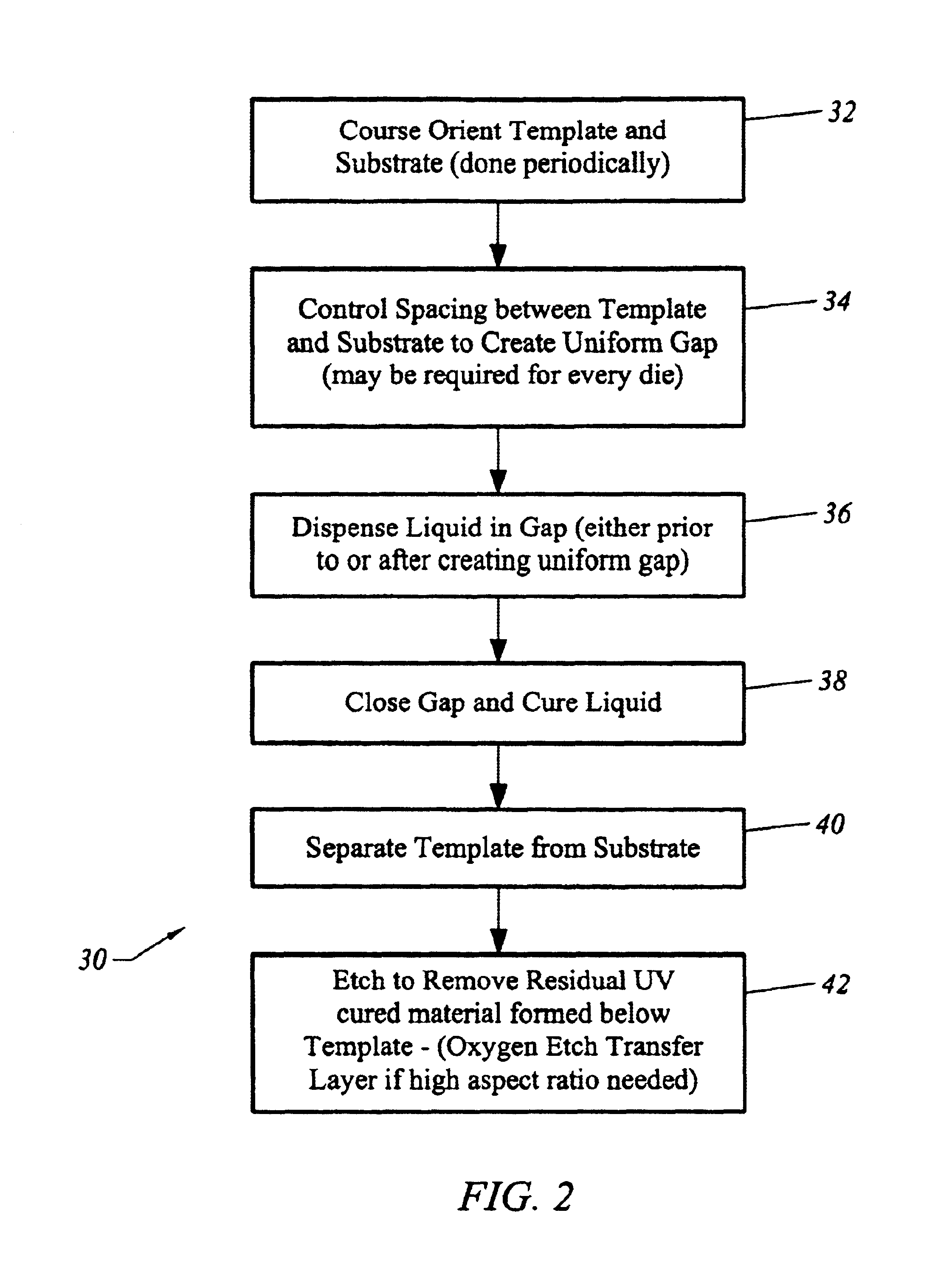
[0021]FIGS. 1A thru 1E illustrate an imprint lithography process according to the invention, denoted generally as 10. In FIG. 1A, a template 12 is orientated in spaced relation to a substrate 14 so that a gap 16 is formed in the space separating template 12 and substrate 14. A surface 18 of template 12 is treated with a thin layer 20 that lowers the template surface energy and assists in separation of template 12 from substrate 14. The manner of orientation including devices for controlling of gap 16 between template 12 and substrate 14 are discussed below. Next, in FIG. 1B, gap 16 is filled with a substance 22 that conforms to the shape of surface 18. Preferably, substance 22 is a liquid so that it fills the space of gap 16 rather easily without the use of high temperatures and gap 16 can be closed without requiring high pressures.

[0022]A curing agent 24, shown in FIG. 1C, is applied to template 12 causing substance 22 to harden and assume the shape of the space defined by gap 16 b...


PUM

PropertyMeasurementUnit
Viscosityaaaaaaaaaa
Electrical conductoraaaaaaaaaa
Electric propertiesaaaaaaaaaa

Abstract

A high-throughput lithography process for creating high-resolution patterns in a polymerizable composition using carefully controlled electric field followed by curing of the polymerizable composition is described. The process involves the use of a template that includes the desired patterns. This template is brought into close proximity to the polymerizable composition on the substrate. An external electric file is applied to the template-substrate interface while maintaining a uniform, carefully controlled gap between the template and substrate. This causes the polymerizable composition to be attracted to the raised portions of the template. By appropriately choosing the various process parameters such as the viscosity of the polymerizable composition, the magnitude of the electric field, and the distance between the template and substrate, the resolution of the structures formed in the liquid may be controlled to conform to that of the template.

Description

BACKGROUND OF THE INVENTION[0001]1. Field of the Invention[0002]This invention generally relates to the area of low cost, high-resolution, high-throughput lithography with the potential to make structures that are below 100 nm in size.[0003]2. Description of the Relevant Art[0004]Optical lithography techniques are currently used to make microelectronic devices. However, these methods are reaching their limits in resolution. Sub-micron scale lithography has been a critical process in the microelectronics industry. The use of sub-micron scale lithography allows manufacturers to meet the increased demand for smaller and more densely packed electronic components on chips. The finest structures producible in the microelectronics industry are currently on the order of about 0.13 μm. It is expected that in the coming years, the microelectronics industry will pursue structures that are smaller than 0.05 μm (50 nm). Further, there are emerging applications of nanometer scale lithography in t...

Claims


Application Information

Patent Timeline
IPC IPC(8): B05D3/14B05D3/06B05D1/40B81C1/00G03F7/00
CPCB05D3/067B05D3/145B29C43/003B81C1/0046B82Y10/00B82Y40/00G03F7/0002B05D1/40B29C2043/025B29C2043/3211
Inventor WILLSON, CARLTON GRANTSREENIVASAN, SIDLGATA V.BONNECAZE, ROGER T.
Owner THE UNIV OF TEXAS SYST
Why Eureka
Try Eureka