Semiconductor device

Inactive Publication Date: 2005-11-15
ROHM CO LTD
View PDF5 Cites 32 Cited by
  • Summary
  • Abstract
  • Description
  • Claims
  • Application Information

AI Technical Summary

Benefits of technology

[0020]According to another aspect of the semiconductor device of the present invention, a structure as claimed in claim 1, wherein the p-type layer and the n-type layer consisting of the bidirectional diode are not planar alignment but are formed alternately in a height direction, and in

Problems solved by technology

The present inventors were devoted to study sufficiently for improving a breakdown strength against a surge and the like of a vertical MOSFET and the like, as a result, it is found out that even if a protective diode such as a zener diode is insert

Method used


Image

  • Semiconductor device
  • Semiconductor device
  • Semiconductor device

Examples


Embodiment Construction

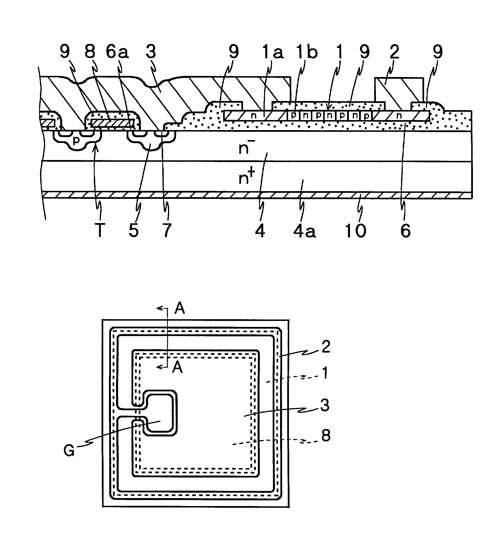
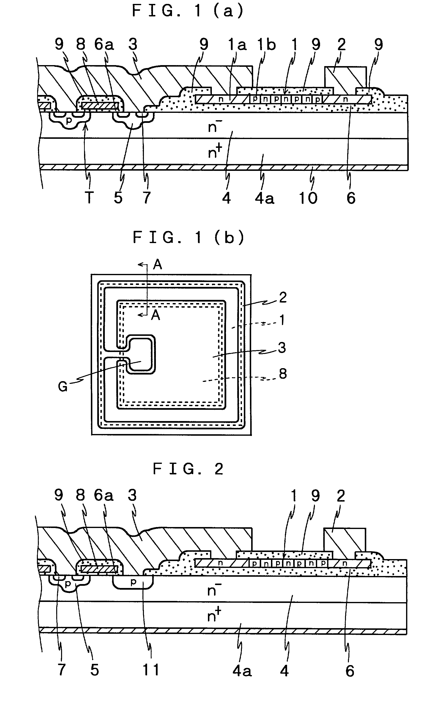
[0031]A description will be given of a semiconductor device according to the present invention with reference to drawings. The semiconductor device according to the present invention comprises a semiconductor layer 4 having a plurality of arranged transistor cells T, as shown in FIG. 1 showing a sectional view of an example for peripheral part of chip of a vertical MOSFET (A—A cross-section of FIG. 1(b)) and an explanation plan view of whole of a chip. A polysilicon film is formed on an insulating film formed on an outer side than the plurality of arranged transistor cells T (the edge side of the chip), and ring-shaped p-type layers 1b and n-type layers 1a are formed alternately and flatly in the polysilicon film to form a protective diode 1. The most outer layer is contacted with a ring-shaped gate wiring 2 successively formed with a gate electrode pad which is composed of metal film such as Al, and the most inner layer is contacted with a source wiring 3 composed of metal film, th...


PUM


Abstract

A plurality of transistor cells (T) are arranged in the semiconductor layer (4). Ring-shaped p-type layers (1b) and n-type layers (1a) composed of polysilicon film are formed alternately on an insulating layer (6) in an outer side than the plurality of transistor cells (T) (the peripheral portion of chip), thereby forming a protective diode (1). The most outer layer of the protective diode (1) is contacted to the gate wiring (2) composed of metal film such as Al, which is formed circularly on the most external layer, and the most inner layer is contacted to the source wiring composed of metal layer, thereby the protective diode is connected between the gate and source of a transistor. As a result of this, the semiconductor device with the protective diode which has the small series resistance, can be formed without enlarging chip area and by using unoccupied space of chip, and realize protection function sufficiently, can be obtained.

Description

FIELD OF THE INVENTION[0001]The present invention relates to a semiconductor device such that a protective diode is connected between a gate and a source of a MOSFET or an insulating gate-type bipolar transistor (IGBT). More specifically, the present invention relates to a semiconductor device which can reduce insertion resistance of the protective diode and increases electrostatic breakdown strength without enlarging a chip area.BACKGROUND ART[0002]Although a vertical MOSFET, for example, has been conventionally used as a switching device having a high-switching speed and a large output, the gate threshold voltage tends to reduce by thinning a gate insulating film. The thinner the insulating film, even a little energy such as a static electricity is easy to insulating broken down. Therefore, a structure in which a protective diode is inserted between a gate and a source to discharge a static electricity has been conventionally used. The protective diode becomes a bidirectional zene...

Claims


Application Information

Patent Timeline
IPC IPC(8): H01L29/66H01L29/78H01L27/02H01L27/06H01L21/336H01L21/822H01L27/04H01L29/06H01L29/739
CPCH01L27/0255H01L27/0629H01L29/66712H01L29/7808H01L29/7811H01L29/0619H01L2924/0002H01L2924/00
Inventor HIGASHIDA, SYOUJITAKAISHI, MASARU
Owner ROHM CO LTD
Why Eureka
Try Eureka