System and method for CMP having multi-pressure zone loading for improved edge and annular zone material removal control

a technology of annular zone and multi-pressure zone, applied in the direction of grinding machine components, manufacturing tools, lapping machines, etc., can solve the problems of inability to solve the problem simultaneously, and inability to meet the requirements of the application

Inactive Publication Date: 2005-11-22
MULTI PLANAR TECH
View PDF34 Cites 19 Cited by
  • Summary
  • Abstract
  • Description
  • Claims
  • Application Information

AI Technical Summary

Problems solved by technology

Wafer to wafer process uniformity as well as intra-wafer planarization uniformity are important issues from the standpoint of producing semiconductor products at a low cost.
As the size of dies increases a flaw in one small area increasing results in rejection of a relatively large circuit so that even small flaws have relatively large economic consequences in the semiconductor industry.
Efforts to simultaneously solve these problems have not heretofore been completely successful.
These inserts are problematic because they frequently result in process variation leading to substrate-to-substrate variation.
This tends to make the initial period of use more like the later period of use, however, unacceptable processes variations are still observed.
Such fabrication increases the costs of the head and of the machine, particularly if multiple heads are provided.
As the size of structures (feature size) on the semiconductor wafer surface have been reduced to smaller and smaller sizes, now typically about 0.2 microns, the problems associated with non-uniform planarization have increased.
When so called hard backed planarization heads, that is heads that press the backside of the semiconductor wafer with a hard...

Method used


Image

  • System and method for CMP having multi-pressure zone loading for improved edge and annular zone material removal control
  • System and method for CMP having multi-pressure zone loading for improved edge and annular zone material removal control
  • System and method for CMP having multi-pressure zone loading for improved edge and annular zone material removal control

Examples


Embodiment Construction

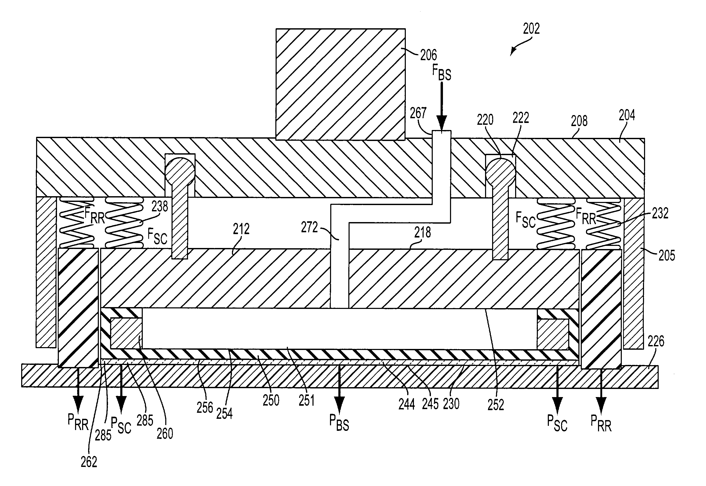
[0037]The inventive structure and method are now described in the context of specific exemplary embodiments illustrated in the figures. The inventive structure and method eliminate many of the problems associated with conventional head designs using polymeric insert between the backside of the wafer and the surface of the wafer subcarrier as well as problems associated with pressure distribution over the surface of the wafer for soft-backed heads. The different forces or pressures impart different loading of the front side surface of the wafer against the polishing pad resulting in a different rate of removal. The pressure applied to a retaining ring similarly alters the loading force of the retaining ring contact surface against the retaining ring and influences material removal at the edge of the wafer. The inventive structure and method replace the insert with a flexible film or membrane adjacent the back side surface of the wafer. In one embodiment, this membrane forms a sealed ...


PUM

PropertyMeasurementUnit
Pressureaaaaaaaaaa
Flexibilityaaaaaaaaaa

Abstract

In one aspect, the invention provides a method for planarizing a circular disc-type semiconductor wafer or other substrate. The method includes the steps of pressing a retaining ring surrounding the wafer against a polishing pad at a first pressure; pressing a first peripheral edge portion of the wafer against the polishing pad with a second pressure; and pressing a second portion of the wafer interior to the peripheral edge portion against the polishing pad with a third pressure. The second pressure may be provided through a mechanical member in contact with the peripheral edge portion; and the second pressure may be a pneumatic pressure against a backside surface of the wafer. Desirably, the pneumatic pressure is exerted through a resilient membrane, or is exerted by gas pressing directly against at least a portion of the wafer backside surface. A carrier or subcarrier for a CMP apparatus that includes: a plate having an outer surface; a first pressure chamber for exerting a force to urge the plate in a predetermined direction; a spacer coupled to a peripheral outer edge of the plate; a membrane coupled to the plate via the spacer and separated from the plate by a thickness of the spacer; and a second pressure chamber defined between the membrane and the plate surface for exerting a second force to urge the membrane in a third predetermined direction. Substrate, such as a semiconductor wafer, processed or fabricated according to the invention.

Description

RELATED APPLICATIONS[0001]This application is a continuation of U.S. patent application Ser. No. 09 / 570,369 filed May 12, 2000 now U.S. Pat. No. 6,558,232.FIELD OF THE INVENTION[0002]This invention pertains generally to systems, devices, and methods for polishing and planarizing semiconductor wafers, and more particularly to systems, devices, and methods utilizing multiple planarization pressure zones to achieving high-planarization uniformity across the surface of a semiconductor wafer.BACKGROUND OF THE INVENTION[0003]As feature size decreases, density increases, and the size of the semiconductor wafer increase, Chemical Mechanical Planarization (CMP) process requirements become more stringent. Wafer to wafer process uniformity as well as intra-wafer planarization uniformity are important issues from the standpoint of producing semiconductor products at a low cost. As the size of dies increases a flaw in one small area increasing results in rejection of a relatively large circuit s...

Claims


Application Information

Patent Timeline
IPC IPC(8): B24B49/16B24B37/04B24B41/06B24B37/30B24B37/32
CPCB24B37/30B24B37/32B24B49/16
Inventor KAJIWARA, JIROMOLONEY, GERARD S.WANG, HUEY-MINGHANSEN, DAVID A.REYES, ALEJANDRO
Owner MULTI PLANAR TECH
Why Eureka
Try Eureka