Method for manufacturing an oriented crystalline semiconductor using a pulsed laser

a technology of oriented crystalline semiconductor and pulsed laser, which is applied in the direction of crystal growth process, polycrystalline material growth, chemistry apparatus and processes, etc., can solve the problems of complex method, inability to control the position or size of each crystal grain, and inability to meet the requirements of crystalline semiconductor material morphology, etc., to achieve the effect of improving the planarity of the crystalline semiconductor material as a film, simplifying the step of forming each projection, and improving the performance of the semiconductor devi

Inactive Publication Date: 2005-12-06
SONY CORP
View PDF4 Cites 7 Cited by
  • Summary
  • Abstract
  • Description
  • Claims
  • Application Information

AI Technical Summary

Benefits of technology

[0008]In an embodiment, the present invention provides a manufacturing method for a crystalline semiconductor material wherein the position, size, and plane orientation of a crystal can be controlled by a simple step, and a crystalline semiconductor material excellent in planarity as a film can be formed.
[0012]According to the manufacturing method for the crystalline semiconductor material of the present invention in an embodiment, the projections are formed on the amorphous or polycrystalline semiconductor layer formed on the substrate. The side wall surface of each projection is substantially perpendicular to the flat surface of the substrate. The height of each projection is set in the range of about 1 nm to less than or equal to about ¼ of the thickness of the semiconductor layer. The lateral dimension of each projection in a direction parallel to the flat surface of the substrate is set in the range of about 3 μm to about 18 μm. Thus, the height of each projection is small, so that the planarity of the crystalline material or the crystalline film is improved. Further, since the side wall surface of each projection is substantially perpendicular to the flat surface of the substrate, the step of forming each projection can be simplified. Further, the crystalline semiconductor material or crystalline film including the crystal grains each having a specific plane orientation with respect to a direction perpendicular to the flat surface of the substrate is formed so that the crystal grains respectively correspond to the projections, by using a pulsed laser to heat the semiconductor layer plural times. By controlling the heating conditions, the size of each crystal grain can be controlled to a desired size, and each crystal grain is preferentially oriented in a specific plane orientation with respect to the direction perpendicular to the flat surface of the substrate.
[0014]According to the manufacturing method for the crystalline semiconductor material of the present invention in an embodiment, the height of each projection is set in the range of 1 nm to less than or equal to ¼ of the thickness of the semiconductor layer. Accordingly, the planarity of the crystalline semiconductor material as a film can be improved, and the performance of the semiconductor device can therefore be improved. Further, since the side wall surface of each projection is substantially perpendicular to the flat surface of the substrate, the step of forming each projection can be simplified. Further, the crystalline semiconductor material including the crystal grains each having a specific plane orientation with respect to a direction perpendicular to the flat surface of the substrate is formed so that the crystal grains respectively correspond to the projections, by using a pulsed laser to heat the semiconductor layer plural times. Accordingly, a crystal grain controlled in size and plane orientation at each projection can be formed.
[0015]According to the manufacturing method for the semiconductor device of the present invention in an embodiment, a crystalline film having crystal grains is formed from the crystalline semiconductor material of the present invention, and a semiconductor element is formed so that each crystal grain included in the crystalline film functions as an operating region. Accordingly, a semiconductor device having semiconductor elements having high performance and uniform characteristics can be fabricated.

Problems solved by technology

In this conventional method, however, it is impossible to control the position or size of each crystal grain.
Accordingly, the device characteristics, reliability, and uniformity of semiconductor elements such as TFTs using a polycrystalline silicon film are considerably inferior to those of semiconductor elements using single-crystal silicon.
However, this method is complicated because the gentle steps must be formed on a resist.
Further, the unevennesses formed on the amorphous silicon film are transferred to a polycrystalline silicon film, causing a degradation in planarity.
As a result, there is a possibility of adverse effect on the characteristics of semiconductor elements formed by using this polycrystalline silicon film.

Method used


Image

  • Method for manufacturing an oriented crystalline semiconductor using a pulsed laser
  • Method for manufacturing an oriented crystalline semiconductor using a pulsed laser
  • Method for manufacturing an oriented crystalline semiconductor using a pulsed laser

Examples


Embodiment Construction

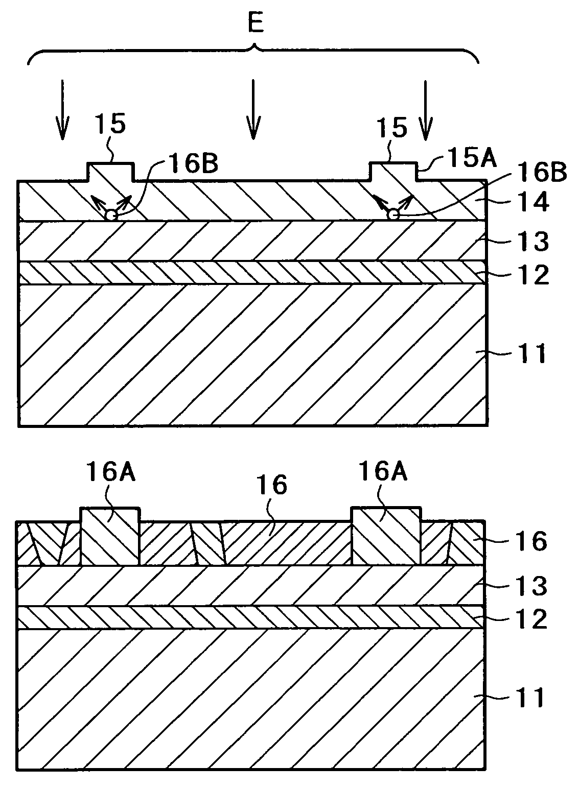
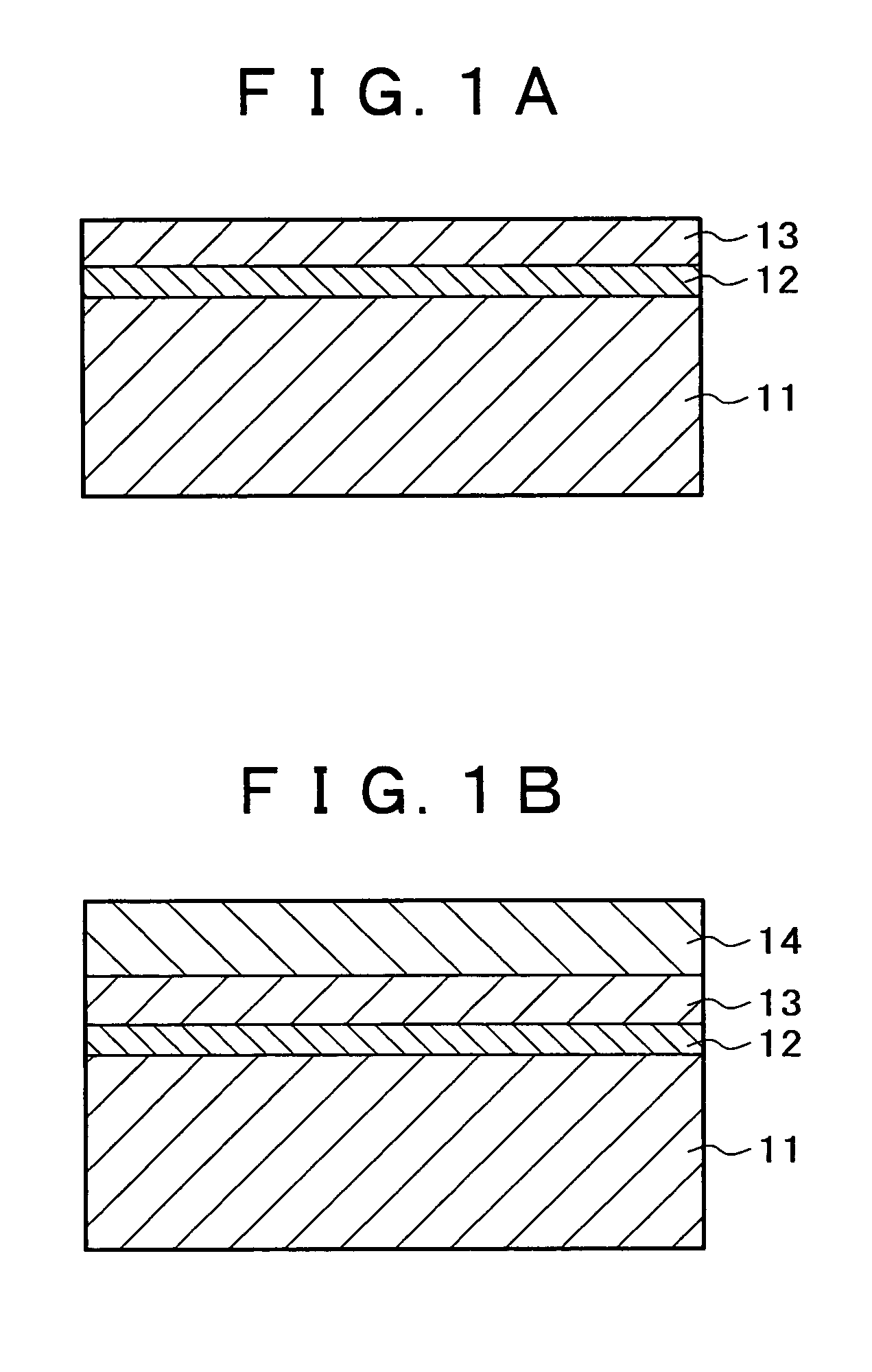
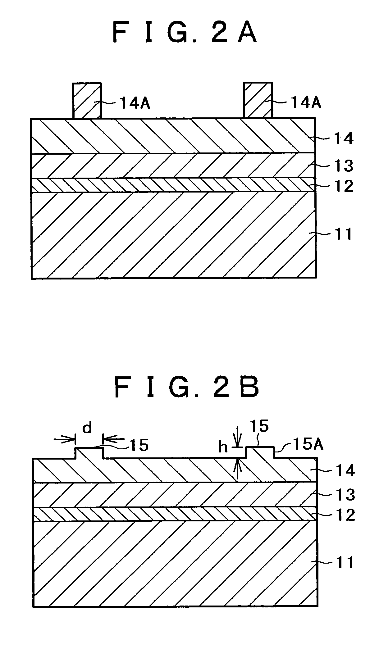
[0023]The present invention relates to a manufacturing method for a crystalline semiconductor material wherein an amorphous or polycrystalline semiconductor layer is heated for crystallization, and also to a manufacturing method for a semiconductor device using the above manufacturing method for the crystalline semiconductor material. Various embodiments of the present invention will now be described in detail below with reference to the drawings.

[0024]FIGS. 1A to 5B except FIG. 3 show the sequential steps of a manufacturing method for a crystalline semiconductor material and a manufacturing method for a semiconductor device subsequent thereto according to a preferred embodiment of the present invention. The manufacturing method for the crystalline semiconductor material includes forming an amorphous or polycrystalline semiconductor layer on a substrate having a flat surface, forming a number of projections on the semiconductor layer, and heating said semiconductor layer a number of...


PUM

PropertyMeasurementUnit
thicknessaaaaaaaaaa
thicknessaaaaaaaaaa
thicknessaaaaaaaaaa

Abstract

A manufacturing method for a crystalline semiconductor material including a plurality of semiconductor crystal grains is provided. The manufacturing method includes forming an amorphous or polycrystalline semiconductor layer on a substrate having a flat surface; forming a plurality of projections each having a side wall surface substantially perpendicular to the flat surface of the substrate, a height set in the range of about 1 nm to less than or equal to about ¼ of the thickness of the semiconductor layer, and a lateral dimension set in the range of about 3 μm to about 18 μm in a direction parallel to the flat surface of the substrate; and heating the semiconductor layer a number of times by using a pulsed laser thereby forming the crystalline semiconductor material including the crystal grains each having a specific plane orientation with respect to a direction perpendicular to the flat surface of the substrate so that the crystal grains respectively correspond to the projections. Accordingly, the position, size, and plane orientation of a crystal can be controlled by a simple step, and a crystalline semiconductor material excellent in planarity as a film can be formed.

Description

CROSS REFERENCES TO RELATED APPLICATIONS[0001]This application claims priority to Japanese Patent Application No. P2003-165119, filed on Jun. 10, 2003, the disclosure of which is incorporated by reference herein.BACKGROUND OF THE INVENTION[0002]The present invention relates to a manufacturing method for a crystalline semiconductor material wherein an amorphous or polycrystalline semiconductor layer is heated for crystallization, and also to a manufacturing method for a semiconductor device using the above manufacturing method for the crystalline semiconductor material.[0003]In recent years, attention has been paid to a technique of forming a semiconductor thin film on a substrate of an amorphous dielectric material such as a glass material or plastic material and fabricating a semiconductor element such as a thin-film transistor (TFT) by using this semiconductor thin film. In actual, such a technique is applied to a switching element, drive circuit, and the like for each pixel in a ...

Claims


Application Information

Patent Timeline
Patent Type & Authority Patents(United States)
IPC IPC(8): C30B13/00C30B29/06H01L21/20H01L21/268H01L21/336H01L21/77H01L21/84H01L27/12H01L29/04H01L29/786H01S3/00
CPCC30B13/00C30B29/06H01L21/2026H01L27/1281H01L29/045H01L29/78675H01L21/02686H01L21/02488H01L21/02502H01L21/02422H01L21/02532H01L21/02609
Inventor NAKANO, KAZUSHIHITSUDA, YUKIHISAFUJINO, TOSHIOSHIOMI, MICHINORISATO, JUNICHI
Owner SONY CORP
Why Eureka
Try Eureka