Thermal management system and method for electronics system

a technology of electronic systems and management systems, applied in lighting and heating apparatus, semiconductor/solid-state device details, domestic cooling apparatus, etc., can solve problems such as increasing heat fluxes, peak heat fluxes in excess of five, and industry has not been able to suspend the laws of physics

Inactive Publication Date: 2005-12-06
THERMAL
View PDF37 Cites 90 Cited by
  • Summary
  • Abstract
  • Description
  • Claims
  • Application Information

AI Technical Summary

Benefits of technology

[0012]A method of managing thermal energy in an electronic system is provided that includes spreading thermal energy generated by one or more devices over a surface that is relatively larger than the devices, thermally coupl

Problems solved by technology

However, the industry has not been able to suspend the laws of physics inasmuch as high computing performance has been accompanied by increased heat generation.
The result of this miniaturization is increasing heat fluxes.
Also, non-uniform heat flux distribution in electronics may result in peak heat fluxes in excess of five times the average heat flux over the entire semiconductor chip surface (˜30 W/cm2).
However, increasing package temperatures will result from the increase in heat dissipation in the package from higher clock speed devices.
As these two conflicting parameters converge, the available thermal budget shrinks.
The lack of understanding of micro-scale heat transfer physics, the requirement of matching the coefficients of thermal expansion (C.T.E.'S) of a semiconductor chip and the thermal energy spreading materials, and the potential adverse effect on conventional packaging practices of integrating heat transfer mechanisms into packages, have largely limited the choice of cooling/spreading techniques at the semiconductor chip and semiconductor package levels to heat conduction.
However, the reduction of these two thermal resistances has now begun to approach the physica

Method used


Image

  • Thermal management system and method for electronics system
  • Thermal management system and method for electronics system
  • Thermal management system and method for electronics system

Examples


Embodiment Construction

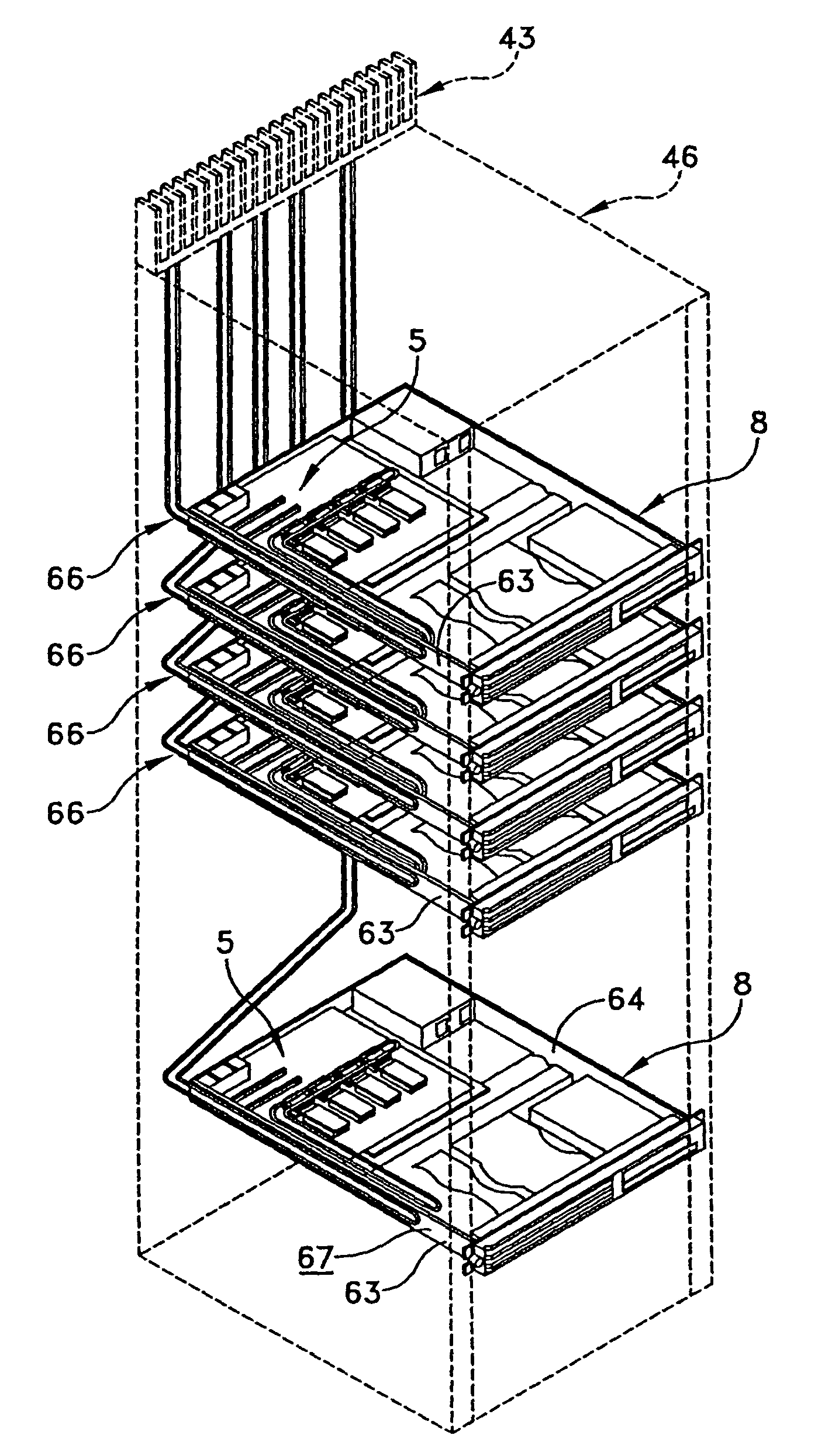
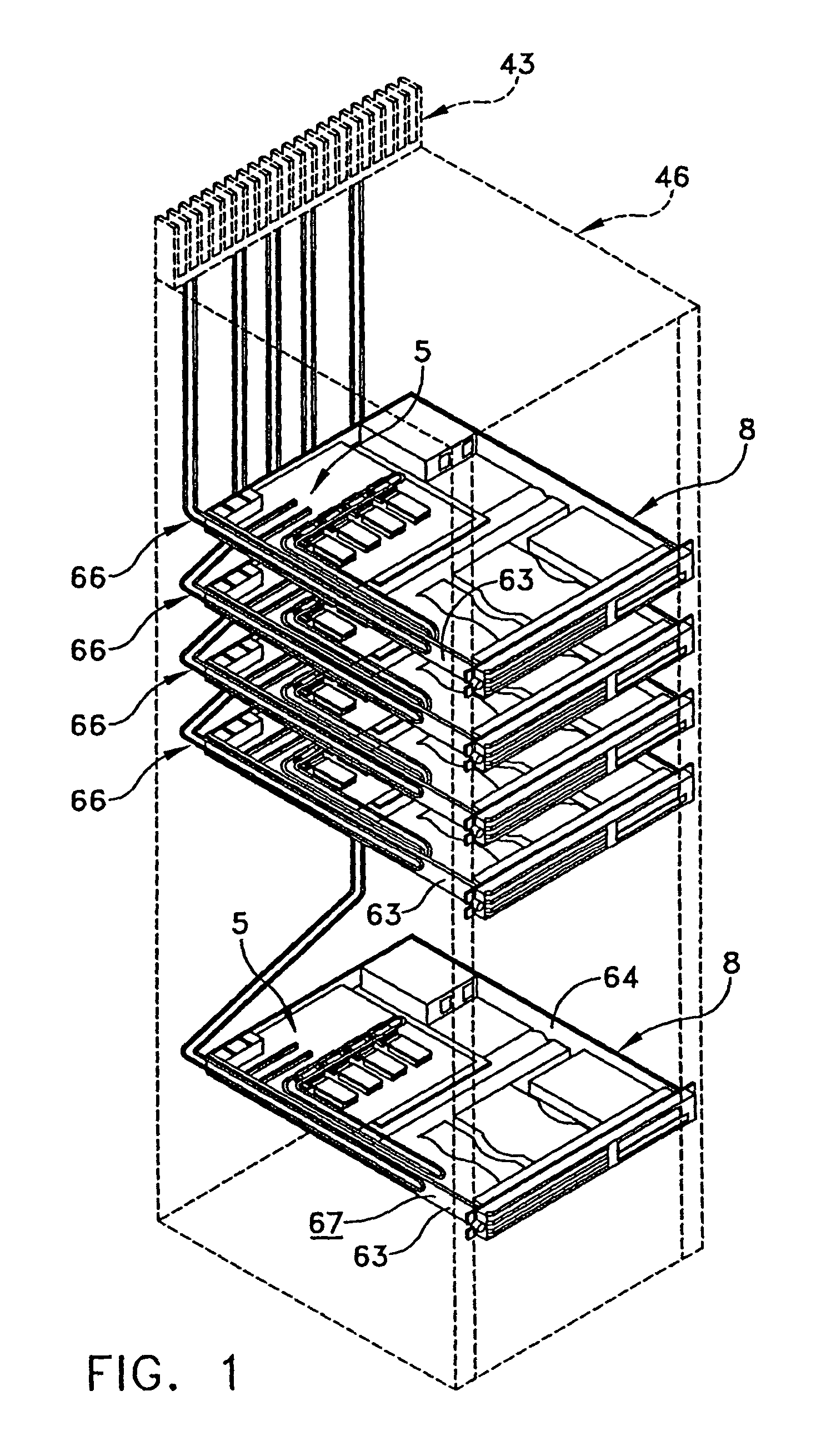
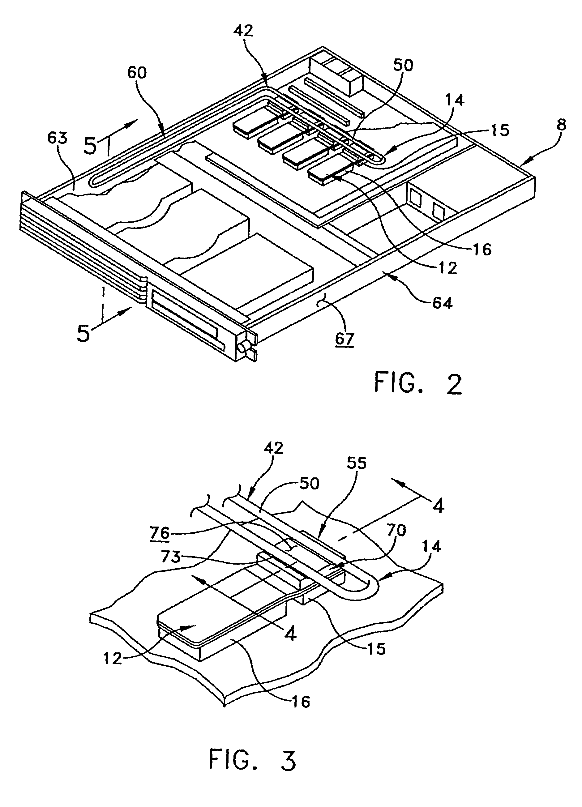
[0019]This description of preferred embodiments is intended to be read in connection with the accompanying drawings, which are to be considered part of the entire written description of this invention. The drawing figures are not necessarily to scale and certain features of the invention may be shown exaggerated in scale or in somewhat schematic form in the interest of clarity and conciseness. In the description, relative terms such as “horizontal,”“vertical,”“up,”“down,”“top” and “bottom” as well as derivatives thereof (e.g., “horizontally,”“downwardly,”“upwardly,” etc.) should be construed to refer to the orientation as then described or as shown in the drawing figure under discussion. These relative terms are for convenience of description and normally are not intended to require a particular orientation. Terms including “inwardly” versus “outwardly,”“longitudinal” versus “lateral” and the like are to be interpreted relative to one another or relative to an axis of elongation, or...


PUM


Abstract

A thermal energy management system is provided having a heat spreading device that is operatively engaged with at least one semiconductor chip and a thermal bus operatively engaged with the heat spreading device so as to transport thermal energy from the heat spreading device to a heat sink. The heat spreading device includes a heat pipe and the thermal bus includes a loop thermosyphon. A second thermal bus may be operatively engaged with the first thermal bus so as to transport thermal energy from the first thermal bus to a heat sink. The second thermal bus may also include a loop thermosyphon. A method of managing thermal energy in an electronic system is also provided that includes spreading thermal energy generated by one or more devices over a surface that is relatively larger than the devices, thermally coupling an evaporator portion of a loop thermosyphon to the surface, and thermally coupling a condensing portion of the loop thermosyphon to a thermal energy sink, e.g., a second loop thermosyphon, convection fin, or cold plate.

Description

[0001]This application is a continuation application of U.S. application Ser. No. 10 / 180,166, filed on Jun. 26, 2002 now U.S. Pat. No. 6,657,121.FIELD OF THE INVENTION[0002]The present invention generally relates to the management of thermal energy generated by electronic systems, and more particularly to a packaging scheme for efficiently and cost effectively routing and controlling the thermal energy generated by various components of an electronic system.BACKGROUND OF THE INVENTION[0003]The electronics industry, following Moore's Law, has seemed to be able to defy the laws of economics by providing ever increasing computing power at less cost. However, the industry has not been able to suspend the laws of physics inasmuch as high computing performance has been accompanied by increased heat generation. Board level heat dissipation has advanced to a point that several years ago was only seen at the system level. The trend toward ever increasing heat dissipation in microprocessor an...

Claims


Application Information

Patent Timeline
IPC IPC(8): H05K7/20
CPCH05K7/20681H05K7/20809H05K7/20818
Inventor GARNER, SCOTT D.
Owner THERMAL
Why Eureka
Try Eureka