Semiconductor device having a lateral MOSFET and combined IC using the same

a technology of lateral mosfet and combined ic, which is applied in the direction of semiconductor devices, diodes, electrical apparatus, etc., can solve the problems of reducing the performance of the lateral parasitic bipolar transistor and the thyristor, prone to malfunction or secondary breakdown, and large area of the lateral surge absorbing section of the bipolar transistor or zener diode constituting the lateral surge absorbing section b>3/b>, so as

Inactive Publication Date: 2005-12-20
FUJI ELECTRIC CO LTD
View PDF9 Cites 24 Cited by
  • Summary
  • Abstract
  • Description
  • Claims
  • Application Information

AI Technical Summary

Benefits of technology

[0011]The present invention provides a semiconductor device for use in integrated intelligent switching devices, double integration type signal input and transfer integrated circuits, and combined power integrated circuits. The device exhibits a high electrostatic discharge withstanding capability and a high surge withstanding capability within the narrow chip area of a lateral MOSFET without the use of complicated insulation structures.

Problems solved by technology

When the device employing the dielectric separation technique is applied to automotive use which requires high ESD, noise, and surge withstanding capability, the area of the bipolar transistor or Zener diode constituting the lateral surge absorbing section 3 inevitably becomes large.
The potential variations are liable to cause malfunctions or secondary breakdown.
However, the countermeasures described above do not substantially improve the characteristics of the lateral parasitic bipolar transistors and the thyristor.
Since the chip area widened to improve the ESD withstanding capability or the surge withstanding capability is hazardous, the dielectric separation technique has been employed more often.

Method used


Image

  • Semiconductor device having a lateral MOSFET and combined IC using the same
  • Semiconductor device having a lateral MOSFET and combined IC using the same
  • Semiconductor device having a lateral MOSFET and combined IC using the same

Examples


first embodiment

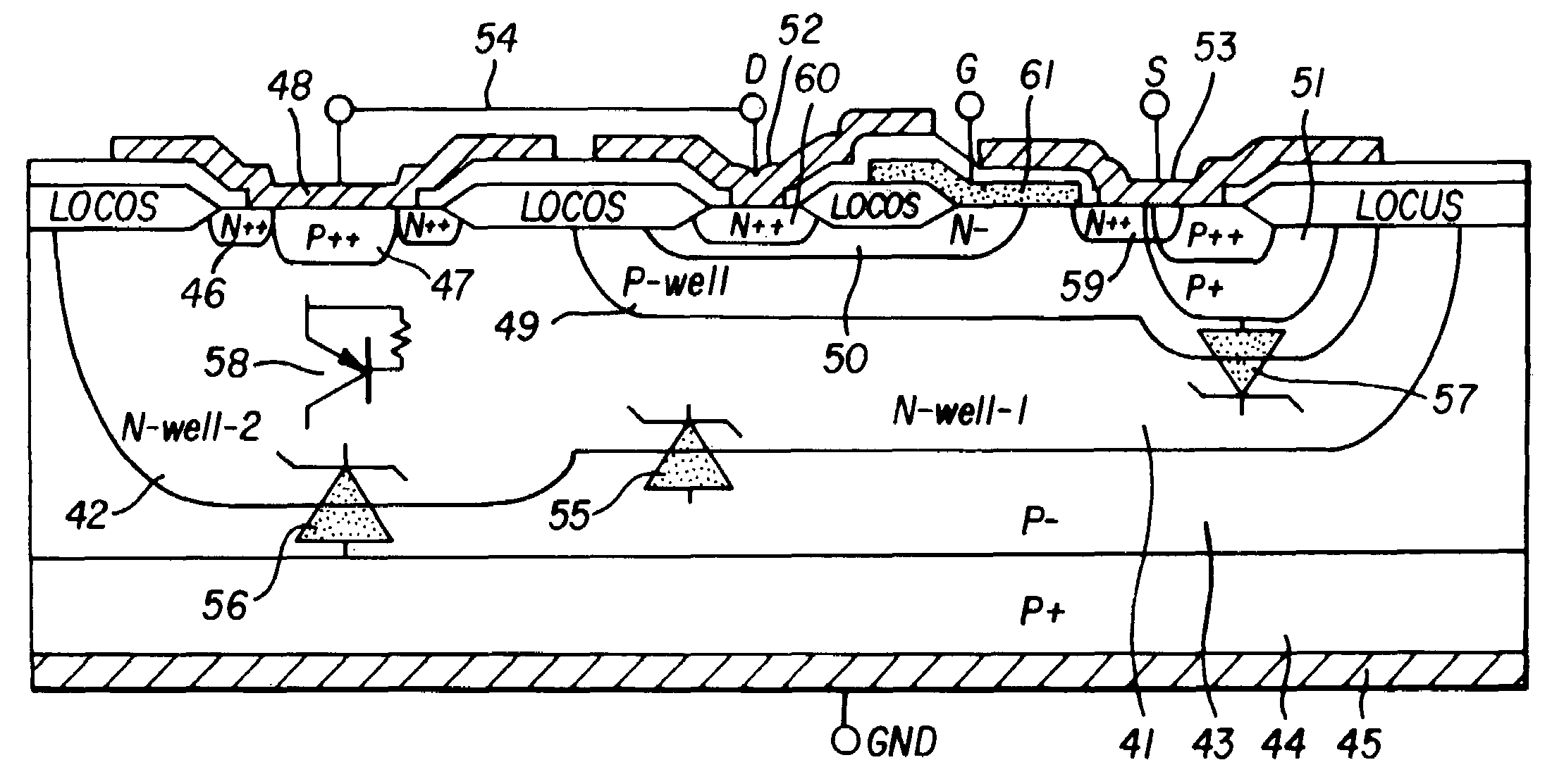
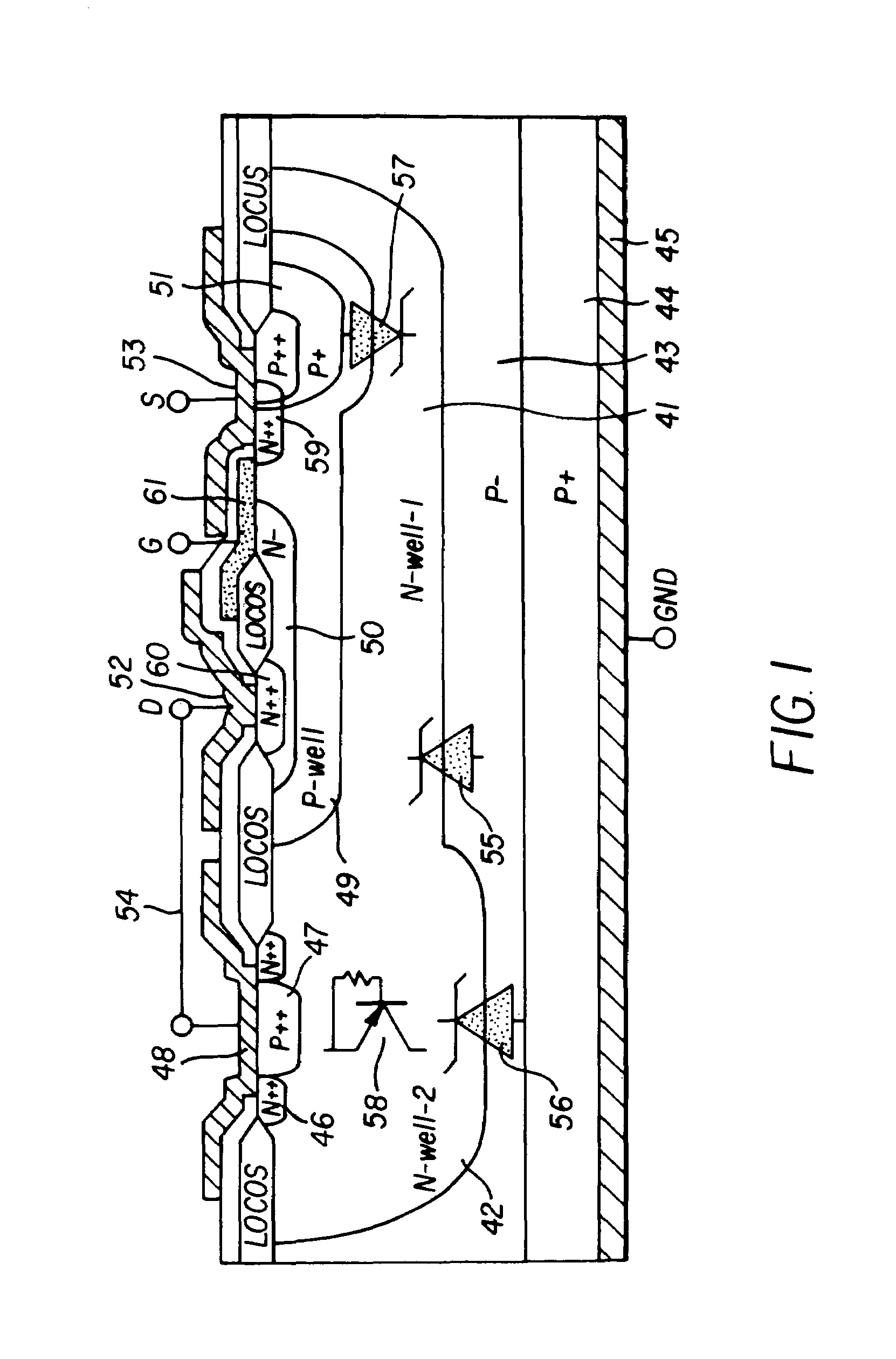
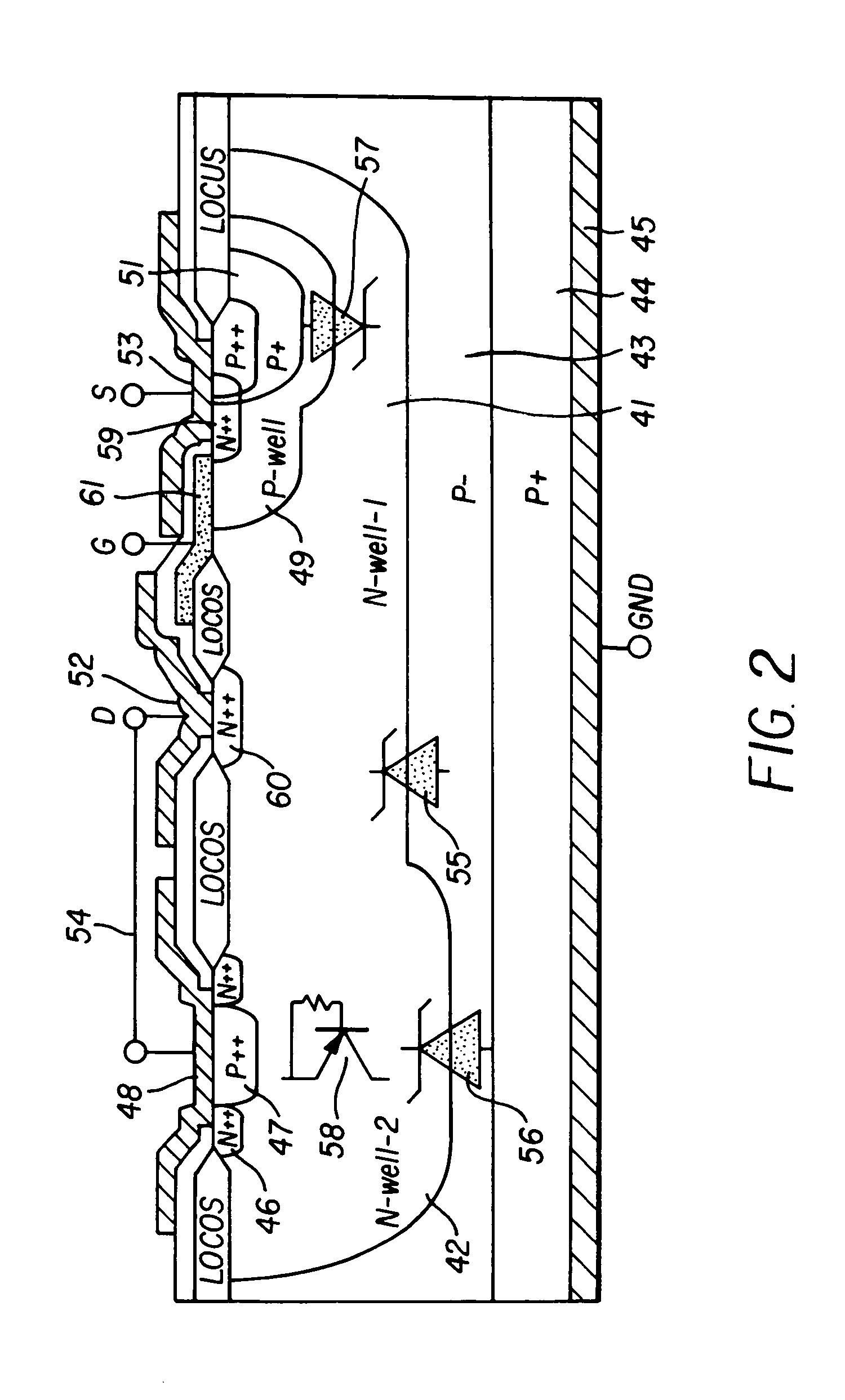
[0058]In the same manner as in the semiconductor device a first p-type well region 49 is in the surface portion of n-type epitaxial layer 73. A lateral MOSFET, formed of an n-type expanded drain region 50, a drain region 60, a drain electrode 52, a p-type region 51, a source region 59, a source electrode 53, a gate oxide film, and a gate electrode 61, is formed in first p-type well region 49.

[0059]Vertical npn bipolar transistor 88 is formed in a second p-type well region 72 formed in the surface portion of n-type epitaxial layer 73. A p-type base region 76 and an n-type emitter region 77 are in the surface portion of second p-type well region 72. Vertical npn bipolar transistor 88 is formed of p-type base region 76, n-type emitter region 77, and the substrate working as a collector region.

[0060]Base region 76 and emitter region 77 are short-circuited to each other by a surface electrode 48. Surface electrode 48 is connected electrically to source electrode 53 of the lateral MOSFET...

tenth embodiment

[0081]FIG. 14 is a block diagram showing a fundamental circuit combination for a combined power IC according to the invention. Referring now to FIG. 14, the combined power IC 220 combines a serial communication circuit 203, a digital signal input and transfer circuit 204, an analog signal input and transfer circuit 205, a high-side intelligent switching device 206 and a low-side intelligent switching device 207. The circuits 203, 204, 205 and the switching deices 206, 207 are connected to the outside via an input-output terminal section 201 exhibiting a high ESD withstanding capability and to a microcomputer 221 via a microcomputer signal connection terminal 202.

[0082]FIG. 15 is a block circuit diagram showing a connection of vertical surge absorbers in the combined power IC of FIG. 14. Referring now to FIG. 15, vertical surge absorbers 219 are connected between the source and drain of a lateral p-channel MOSFET 209 and between the source and drain of a lateral n-channel MOSFET 210 ...


PUM


Abstract

A semiconductor device realizes a high electrostatic discharge withstanding capability and a high surge withstanding capability within the narrow chip area of a lateral MOSFET used in integrated intelligent switching devices, double-integration-type signal input and transfer IC's, and combined power IC's. The semiconductor device includes a vertical bipolar transistor in which a base is electrically connected to an emitter and a collector, and a lateral MOSFET including a drain electrode connected to a surface electrode. The vertical bipolar transistor absorbs electrostatic discharge or surge energy when a high electrostatic discharge voltage or a high surge voltage is applied and limits the electrostatic discharge voltage or the surge voltage to be lower than the breakdown voltage of the lateral MOSFET.

Description

BACKGROUND OF INVENTION[0001]The present invention relates to a semiconductor device exhibiting a high electrostatic-discharge withstanding capability (hereinafter referred to as an “ESD withstanding capability”) and a high surge withstanding capability. Specifically, the present invention relates to a semiconductor device constituting an integrated intelligent switching device, a combined signal input and transmission IC or a combined power IC.[0002]Integrated intelligent switching devices, which incorporate a plurality of power semiconductor devices and a driving and controlling circuit on a same chip, have been used in on-vehicle electric equipment, various kinds of industrial equipment, motor controllers, office automation (OA) equipment, mobile (portable) equipment, household appliances and such equipment which are required to exhibit high noise withstanding capabilities including a high ESD withstanding capability and an electromagnetic compatibility (hereinafter referred to a...

Claims


Application Information

Patent Timeline
Patent Type & Authority Patents(United States)
IPC IPC(8): H01L27/04H01L21/822H01L21/8222H01L21/8234H01L21/8248H01L21/8249H01L27/02H01L27/06H01L29/78
CPCH01L29/7801H01L29/7835H01L27/0251H01L2924/0002H01L2924/00H01L29/7817H01L29/7821H01L29/7816
Inventor YOSHIDA, KAZUHIKOICHIMURA, TAKESHIFUJIHIRA, TATSUHIKOKUMAGAI, NAOKI
Owner FUJI ELECTRIC CO LTD
Why Eureka
Try Eureka