

Electronic circuit board
a technology of electronic circuit board and circuit board, which is applied in the direction of electrical apparatus contruction details, printed circuit non-printed electric components association, instruments, etc., can solve the problems of difficult efficient light supply, achieve the effect of increasing the wiring size, increasing the speed, and facilitating the easy mounting
- Summary
- Abstract
- Description
- Claims
- Application Information
AI Technical Summary
Benefits of technology
Problems solved by technology
Method used
Image

Examples
embodiment 1
(Embodiment 1)
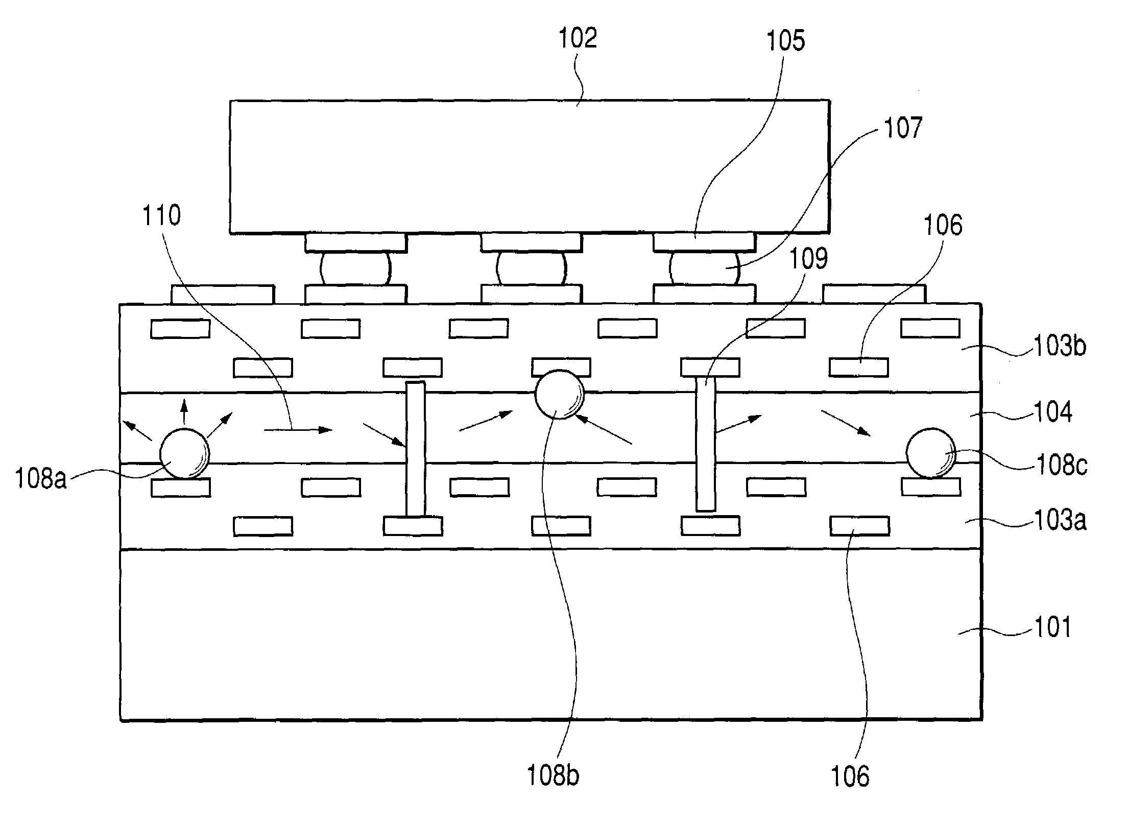
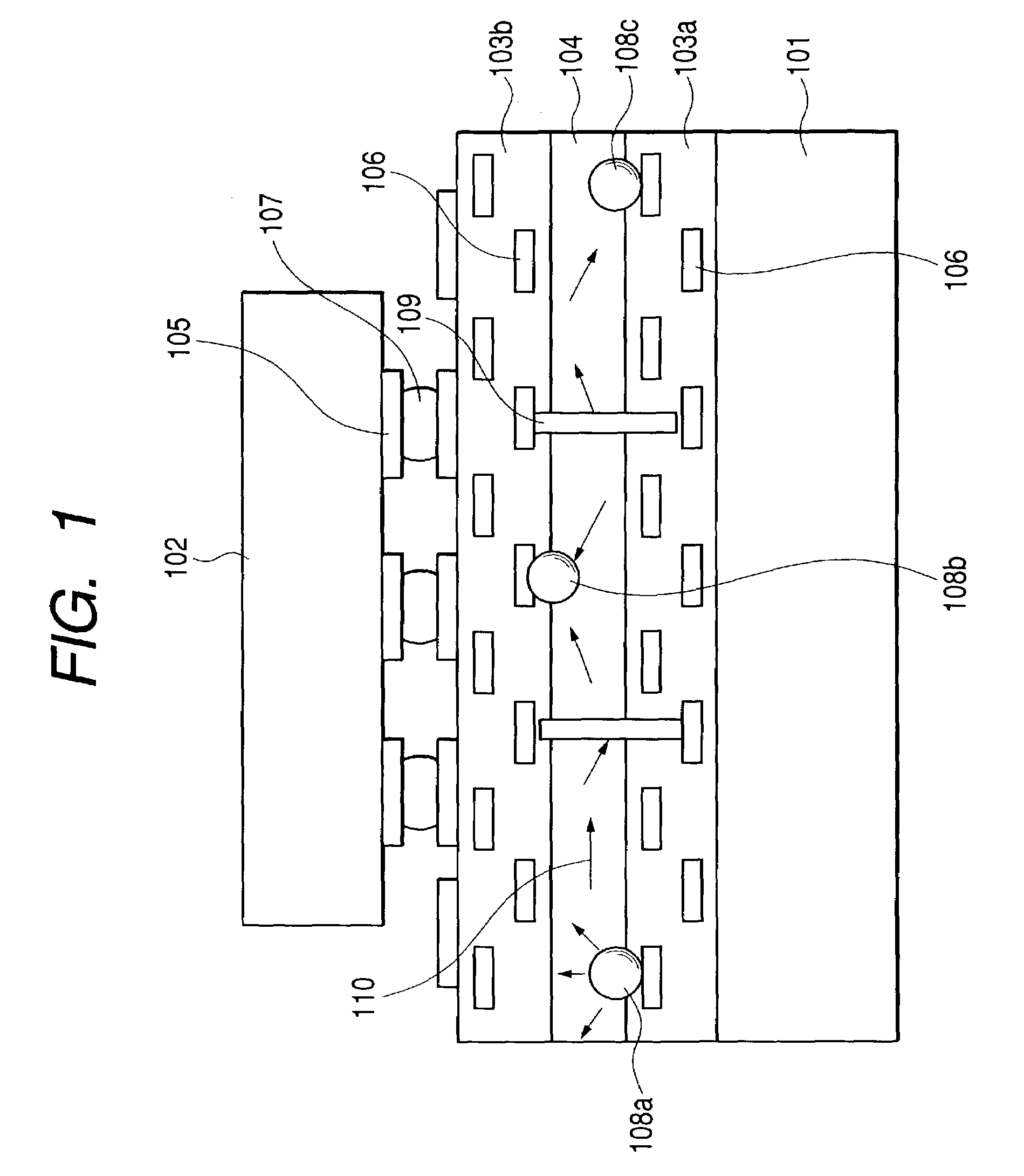
[0061]FIG. 1 is a sectional view of the electronic circuit board according to the present invention. Photonic ball ICs are provided at upper and lower interfaces of an optical wiring layer.
[0062]In FIG. 1, the reference numeral 101 represents a circuit board base, 103a and 103b electrical wiring layers, and 104 a film-shaped optical wiring layer sandwiched between the electrical wiring layers. The reference numeral 102 denotes an IC chip mounted on the surface of the electrical wiring layer 103b by means of bumps (e.g., solder balls) 107. The reference numerals 108a through 108c represent photonic ball ICs that are mounted at interfaces between the electrical wiring layers 103a and 103b and the optical wiring layer 104. The reference numeral 106 represents micro-strip lines formed in the electrical wiring layers or on the surface thereof. The reference numeral 105 represents electrode pads electrically connected to them. The reference numeral 109 represents vias that m...
embodiment 2
(Embodiment 2)
[0101]FIG. 6 schematically shows a sectional view of a second embodiment of the present invention.
[0102]Differences from the first embodiment are: (1) optical wiring layers 104a and 104b are multilayered; (2) no circuit board base is used; and (3) electronic devices 102a and 102b are mounted on both surfaces. The mutually corresponding members in FIGS. 6 and 1 are designated by the same reference numerals.
(Common Points)
[0103](1) Each of the optical wiring layers 104a and 104b transmits data by diffusing an optical signal two-dimensionally.
[0104](2) vias are to connect electrical wiring layers 103a through 103c with each other.
[0105]The embodiment is briefly supplemented as follows.[0106]According to embodiment 1, the photonic ball ICs 108 are mounted at specified positions on the surface of the electrical wiring layer 103a (e.g., PMMA).[0107]The optical wiring layer 104a is formed on the surface thereof.[0108]The photonic ball ICs 108 are mounted on the second electri...
embodiment 3
(Embodiment 3)
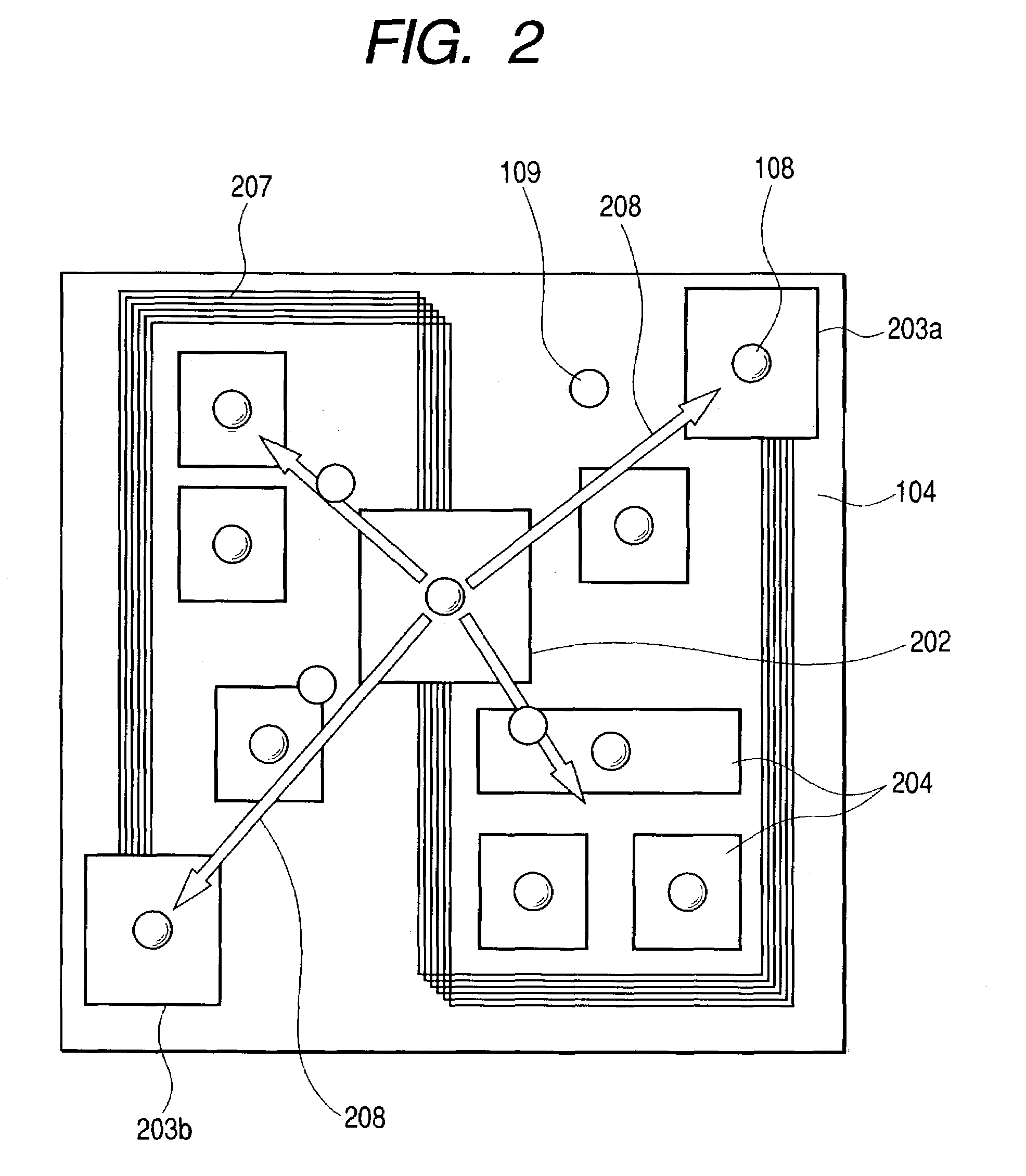
[0112]The ball IC is also used as a scatterer.
[0113]FIG. 7 is a schematic diagram for explaining the third embodiment. The mutually corresponding members in FIGS. 7 and 1 are designated by the same reference numerals.
[0114]Main differences from the first embodiment are as follows.
[0115](1) Optical scatterers 111a through 111c are arranged near the photonic ball ICs 108a through 108c.
[0116](2) When light is emitted, each optical scatterer functions as a scatterer to diffuse the light throughout the optical wiring layer 104.
[0117](3) When light is received, each optical scatterer functions as a condenser to efficiently condenses the light to the light receiver just above.
[0118]The embodiment is briefly supplemented as follows.[0119]According to embodiment 1, the photonic ball ICs 108a and 108c and the optical scatterer or condenser 111b are mounted at specified positions on the surface of the electrical wiring layer 103a (e.g., PMMA).[0120]The optical wiring layer 104 i...
PUM
 Abstract
Description
Claims
Application Information