

Method for making a microelectronic interposer
a micro-electronic interposer and interposer technology, applied in the direction of etching metal masks, fixed connections, coupling device connections, etc., can solve the problems of weak electrical interconnections formed by deposited conductive materials in such drilled holes, high depth to diameter ratio, and large space consumed in assembly, so as to facilitate vertical movement of peripheral parts
- Summary
- Abstract
- Description
- Claims
- Application Information
AI Technical Summary
Benefits of technology
Problems solved by technology
Method used
Image

Examples
Embodiment Construction
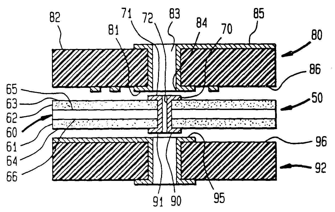
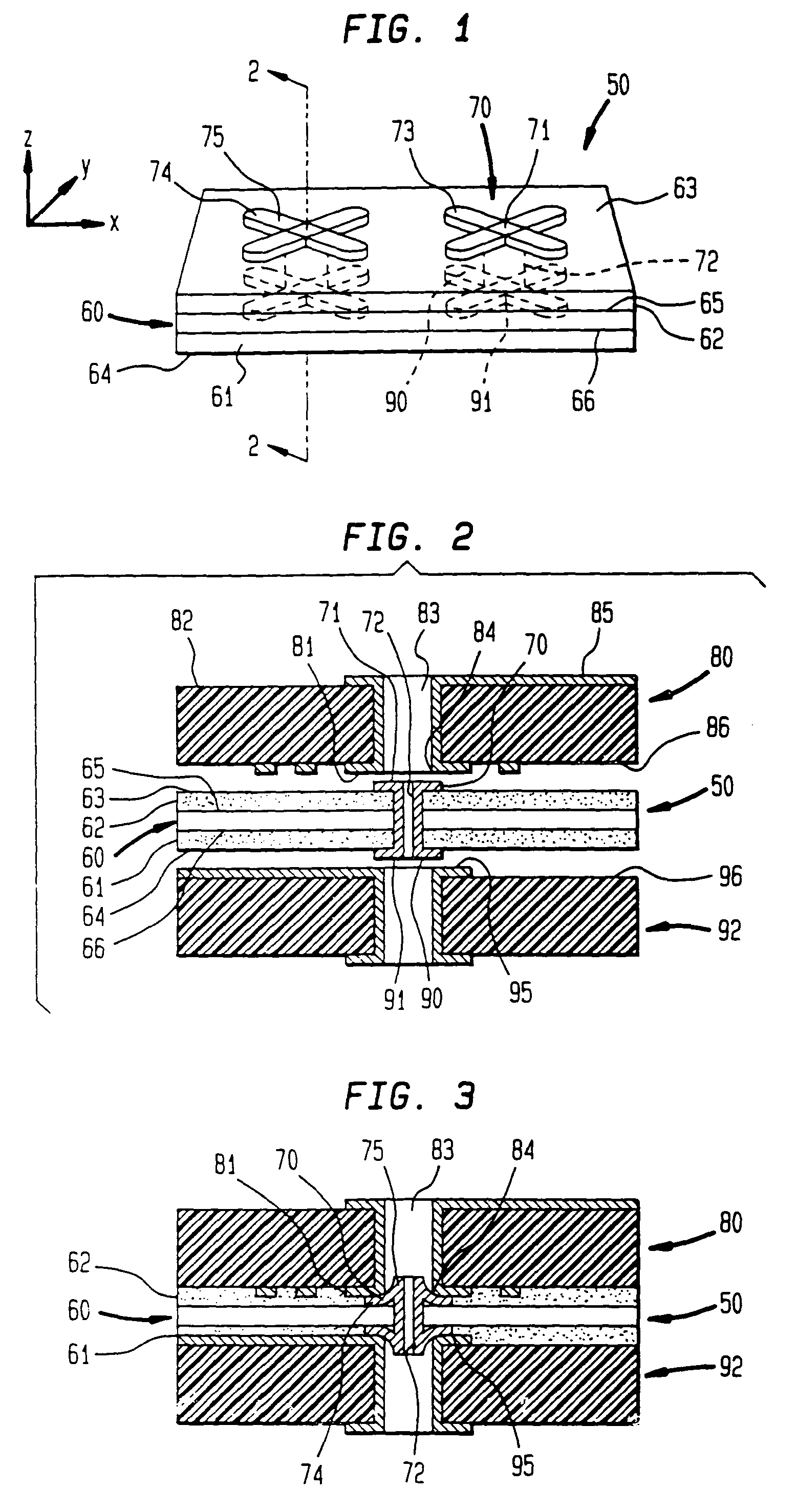
[0061]An interposer according to one embodiment of the invention, shown in FIG. 1, has a body 60 with a first major surface 65. The body 60 may be formed of a dielectric material such as polyimide, or of another non-conducting material. The top surface 65 of the body 60 extends in horizontal directions; i.e., directions x, y as shown in FIG. 1. A plurality of conductors 72 extend vertically, or in the z direction, into the body. In the preferred embodiment shown in FIG. 1, the conductors 72 extend through the body 60. The conductors 72 may be elements formed by conductively plating vertical holes extending into the body 60 from the first surface 65. The conductors are formed of a structural conductive material such as copper, gold, tin or alloys thereof.
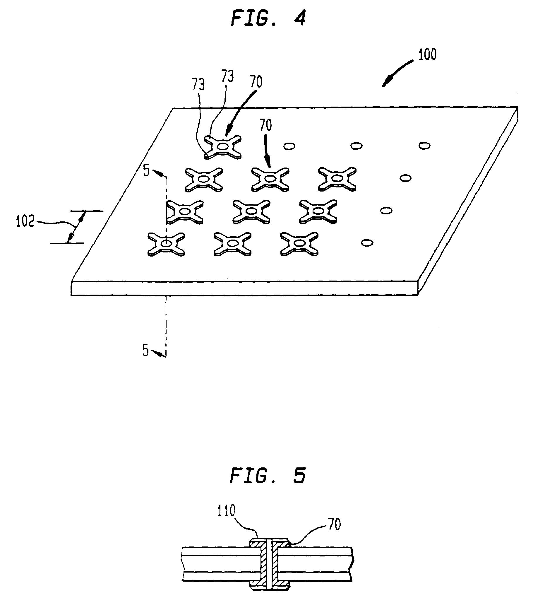
[0062]Each of the conductors 72 has a first end 71 positioned on or above the first major surface 65 of the body 60. Extending radially outward from the end 71 of the conductor is a contact 70. In the preferred embodiment shown in FI...
PUM
| Property | Measurement | Unit |
|---|---|---|
| Electrical conductivity | aaaaa | aaaaa |
| Adhesivity | aaaaa | aaaaa |
Abstract
Description
Claims
Application Information