Image sensor and method for fabricating the same
a technology of image sensor and crystalline defect, which is applied in the field of image sensor, can solve the problems of image sensor abnormal state, limited attempt, and crystalline defect mainly at the edge, and achieve the effect of suppressing the generation of dark curren
- Summary
- Abstract
- Description
- Claims
- Application Information
AI Technical Summary
Benefits of technology
Problems solved by technology
Method used
Image

Examples
Embodiment Construction
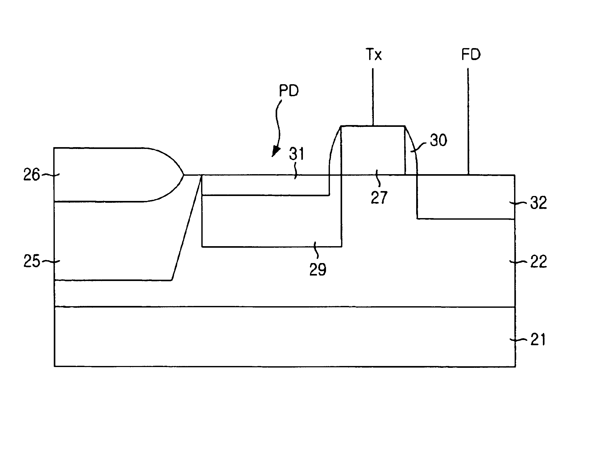
[0040]FIG. 3 is a plane view showing a complementary metal-oxide semiconductor device (hereinafter referred as to CMOS) image sensor in accordance with a first preferred embodiment of the present invention. The-CMOS image sensor shown in FIG. 3 includes a photodiode area (hereinafter referred as to PD), a gate electrode of a transfer transistor Tx and a floating diffusion area (hereinafter referred as to FD).
[0041]On a predetermined place of a substrate 21, an active area including the PD, the FD having a smaller area than the PD and a channel area ch having a bottle-neck structure that connects the PD and the FD is formed.
[0042]Then, a field oxide layer 26 for isolating electrically the active area is formed. A field stop layer 25 having a greater area than the field oxide layer 26 as being extended towards the active area with a first predetermined distance is formed beneath the field oxide layer 26.
[0043]Also, a gate electrode 27 having one side superposed entirely on one side of...
PUM
 Abstract
Description
Claims
Application Information