Gallium-nitride based light-emitting diode epitaxial structure

a light-emitting diode and gallium-nitride technology, applied in the field of epitaxial structure of gallium-nitride-based light-emitting diodes, can solve the problems of gan-based led having inferior device characteristics, reducing the external quantum efficiency of gan-based led, and si-doped barrier layers also have side effects

Active Publication Date: 2005-12-27
FORMOSA EPITAXY INCORPORATION +1
View PDF8 Cites 19 Cited by
  • Summary
  • Abstract
  • Description
  • Claims
  • Application Information

AI Technical Summary

Benefits of technology

[0006]The present invention provides a number of epitaxial structures for the GaN-based LED so that the limitations and disadvantages from the prior arts can be obviated practically.

Problems solved by technology

However, the Si-doped barrier layers also have a side effect.
This would apparently decrease the external quantum efficiency of the GaN-based LED.
Due to the piezoelectric effect, excessive stress would therefore be developed among the epitaxial structure of the GaN-based LED, causing the GaN-based LED to have inferior device characteristics.

Method used


Image

  • Gallium-nitride based light-emitting diode epitaxial structure
  • Gallium-nitride based light-emitting diode epitaxial structure
  • Gallium-nitride based light-emitting diode epitaxial structure

Examples


first embodiment

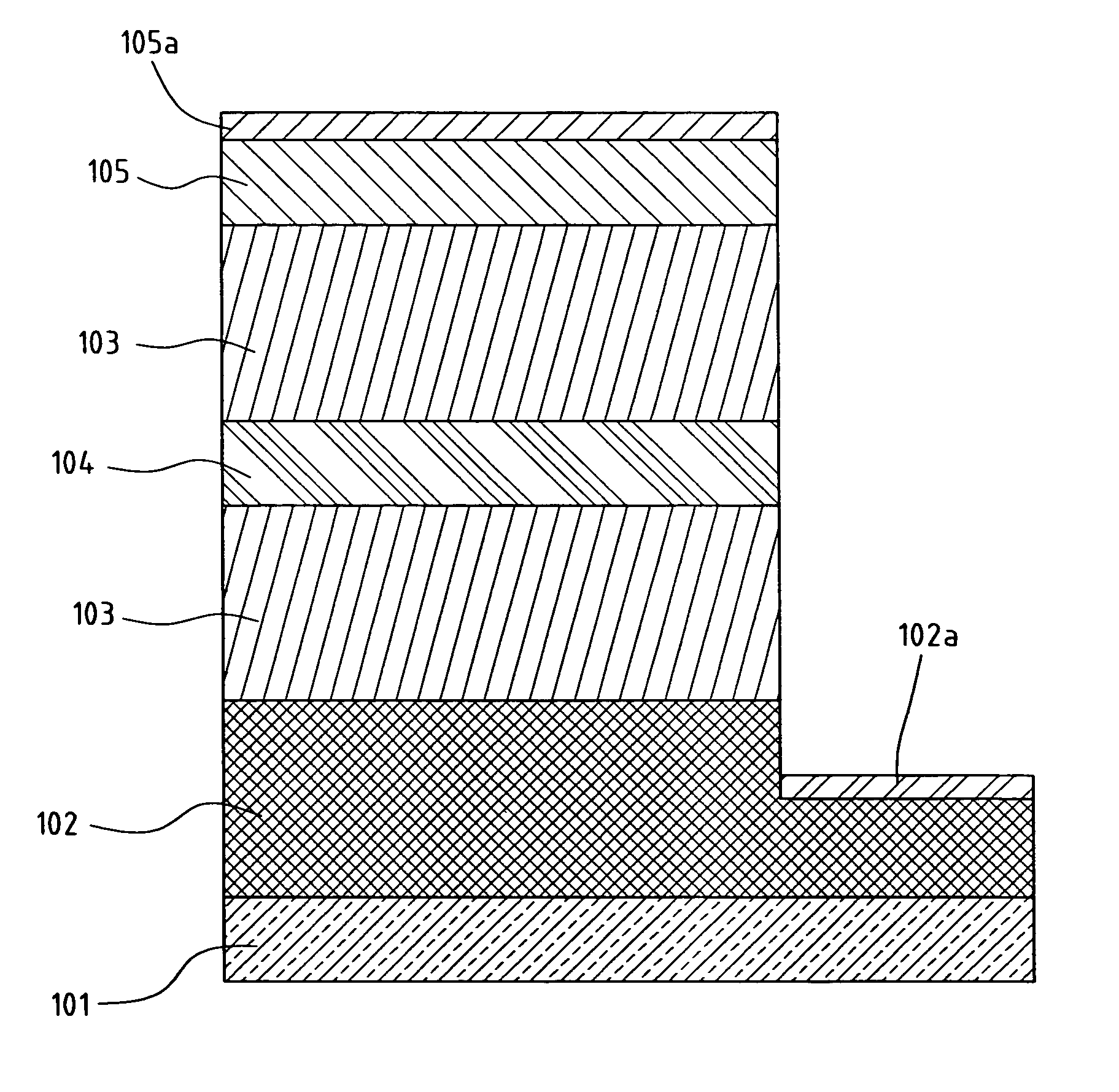
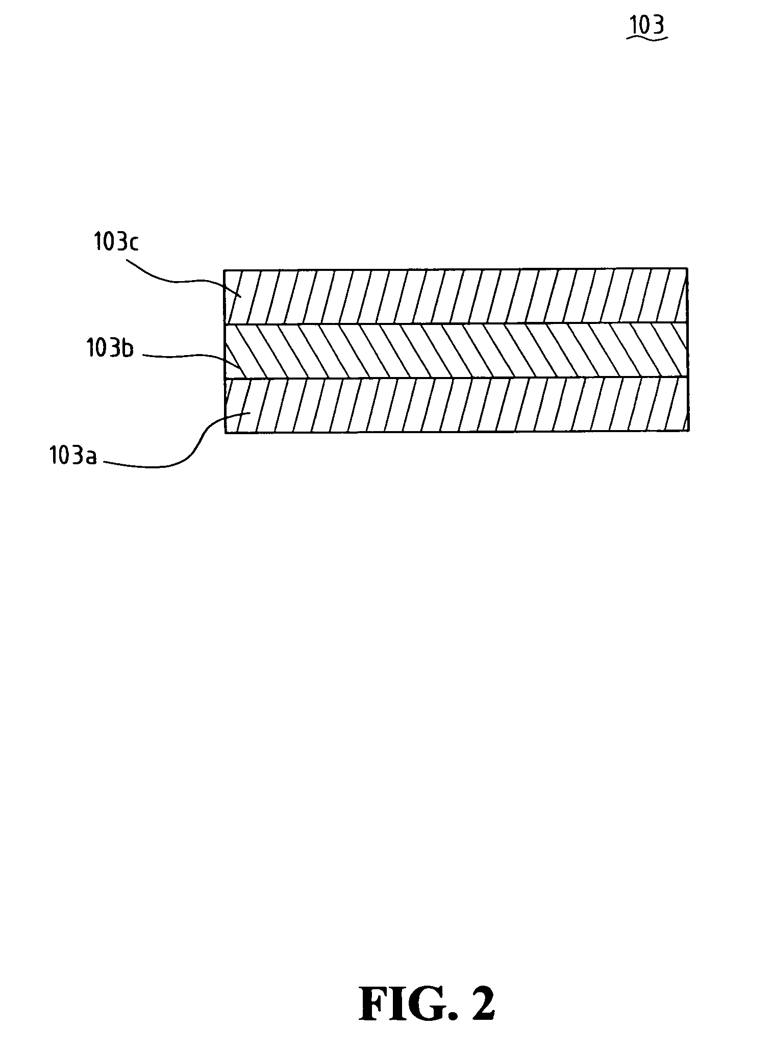
[0015]FIG. 1 is a schematic diagram showing the epitaxial structure of the GaN-based LED according to present invention. On the other hand, the inner structure of the barrier layer within the epitaxial structure is depicted in FIG. 2.

[0016]As shown in FIG. 1, the GaN-based LED is formed by stacking a n-type contact layer 102, a lower barrier layer 103, an active layer 104, an upper barrier layer 103, a p-type contact layer 105, sequentially in this order from bottom to top on an upper side of a substrate 101.

[0017]The substrate 101 is made of C-plane, R-plane, or A-plane aluminum-oxide monocrystalline (or sapphire), or an oxide monocrystalline having a lattice constant compatible with that of nitrides. The substrate 101 can also be made of SiC (6H—SiC or 4H—SiC), Si, ZnO, GaAs, or MgAl2O4. Generally, the most common material used for the substrate 101 is sapphire or SiC. On an upper side of the substrate 101, an n-type contact layer 102 is formed and made of an n-type GaN material. ...

second embodiment

[0024]FIG. 4 is a schematic diagram showing the epitaxial structure of the GaN-based LED according to present invention.

[0025]As shown in FIG. 4, the GaN-based LED contains a substrate 101, a n-type contact layer 102, multiple barrier layers 103 and multiple active layers 104 alternately stacked upon each other from bottom to top with a barrier layer 103 at the bottom and an active layer 104 at the top, another barrier layer 103 on top of the topmost active layer 104, and a p-type contact layer 105, sequentially stacked in this order. The substrate 101, the n-type contact layer 102, the barrier layer 103, the active layer 104, and the p-type contact layer 105 are all formed in processes identical to those of the first embodiment.

[0026]Please be noted that each of the AlGaInN layers 103a and 103c within the barrier layers 103 has a wider band gap than that of the active layer 104.

[0027]Each of the barrier layers 103 within the second embodiment of the present invention as depicted in...


PUM


Abstract

An epitaxial structure for the GaN-based LED is provided. The GaN-based LED uses a substrate usually made of sapphire or silicon-carbide (SiC). On top of the substrate, the GaN-based LED contains an n-type contact layer made of an n-type GaN-based material. On top of the n-type contact layer, the GaN-based LED further contains a lower barrier layer covering part of the surface of the n-type contact layer. A negative electrode is also on top of and has an ohmic contact with the n-type contact layer in an area not covered by the lower barrier layer. On top of the lower barrier layer, the GaN-based LED then further contains an active layer made of aluminum-gallium-indium-nitride, an upper barrier layer, a p-type contact layer made of a magnesium (Mg)-doped GaN material, and a positive electrode having an ohmic contact with the p-type contact layer, sequentially stacked in this order from bottom to top. Within this structure, each of the barrier layers further contains, from bottom to top, a first AlGaInN layer, a SiN layer, and a second AlGaInN layer.

Description

BACKGROUND OF THE INVENTION[0001]1. Field of the Invention[0002]The present invention relates to the gallium-nitride based light-emitting diode, and in particular to the epitaxial structure of the gallium-nitride based light-emitting diode.[0003]2. The Prior Arts[0004]Gallium-nitride (GaN) based light-emitting diodes (LEDs) has been the research and development focus in the academic arena and in the industries in recent years. A conventional practice for the GaN-based LEDs is to use the multi-quantum well (MQW) structure in the GaN-based LED's active layer, which is interposed between barrier layers made of Si-doped GaN. The barrier layers effectively confine the electrons and holes inside the active layer and, thereby, increase the possibility of forming the electron-hole pairs inside the active layer. This in turn increases the internal quantum efficiency and decreases the operating voltage as well of the GaN-based LED. However, the Si-doped barrier layers also have a side effect....

Claims


Application Information

Patent Timeline
Patent Type & Authority Patents(United States)
IPC IPC(8): H01L29/06H01L31/0328H01L33/06H01L33/32
CPCB82Y20/00H01L33/32H01L33/06
Inventor YU, CHENG-TSANGTU, RU-CHINWU, LIANG-WENWEN, TZU-CHICHIEN, FEN-REN
Owner FORMOSA EPITAXY INCORPORATION
Why Eureka
Try Eureka