

Semiconductor device with CMOS-field-effect transistors having improved drain current characteristics
a field-effect transistor and semiconductor technology, applied in semiconductor devices, semiconductor/solid-state device details, electrical apparatus, etc., can solve the problems of increasing the installation cost of new manufacture apparatuses, crystal dislocation, and high energy dispersion, so as to increase the operating speed of field-effect transistors and increase the mobility.
- Summary
- Abstract
- Description
- Claims
- Application Information
AI Technical Summary
Benefits of technology
Problems solved by technology
Method used
Image

Examples
first embodiment
[0142]the present invention will be described below by referring to FIGS. 1 to 3, 8, and 31.
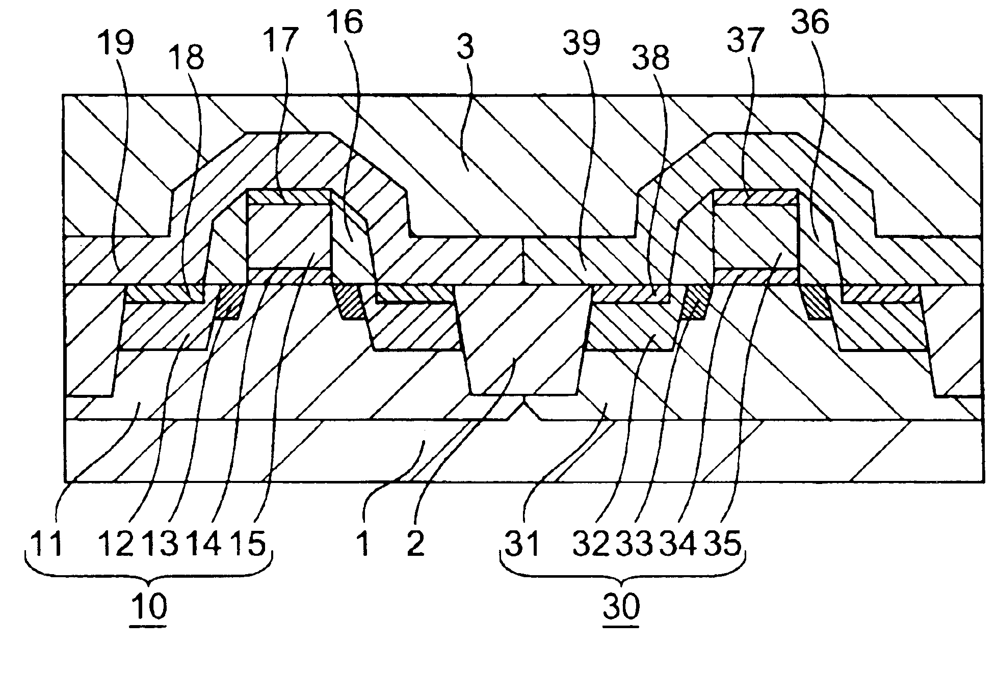
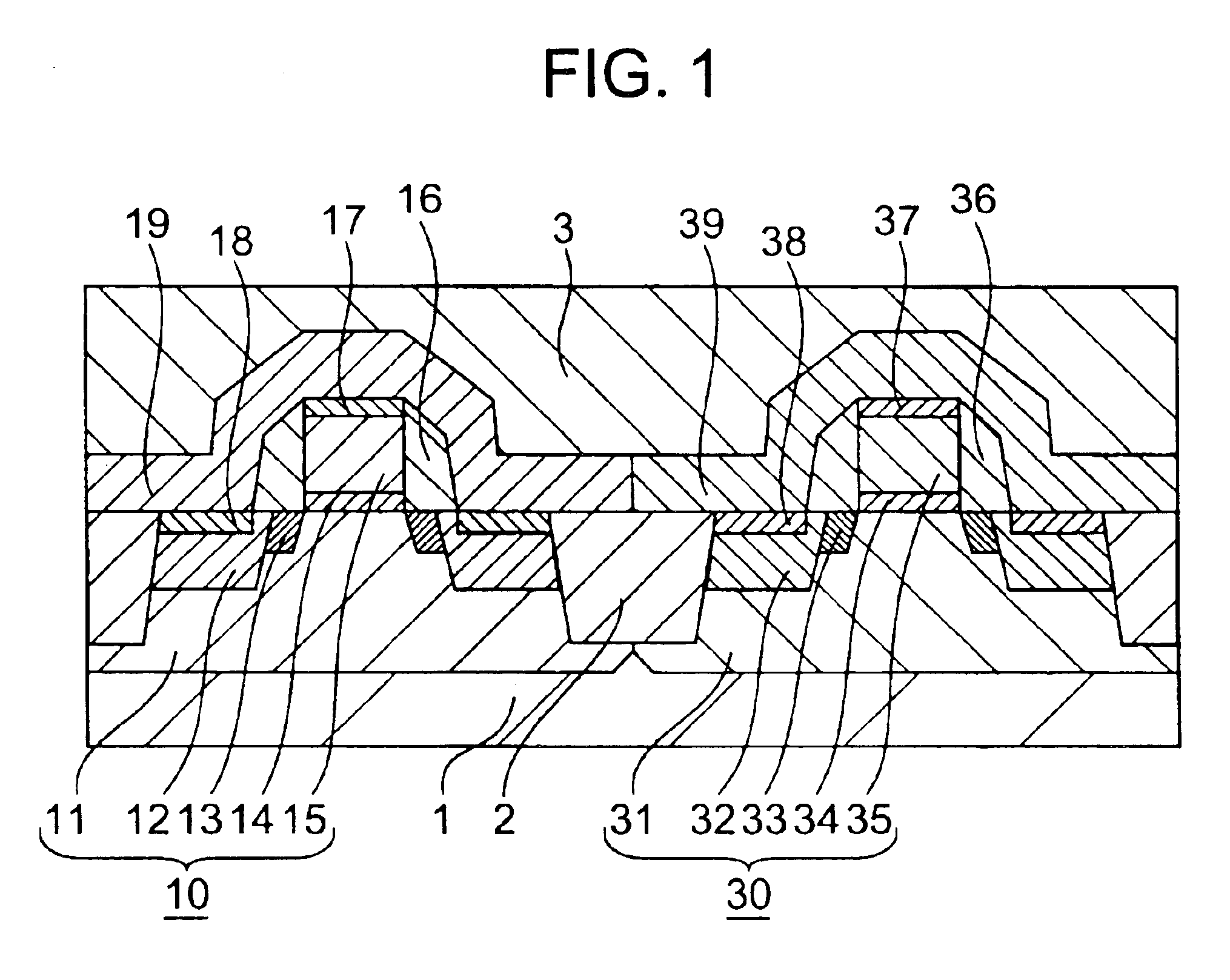
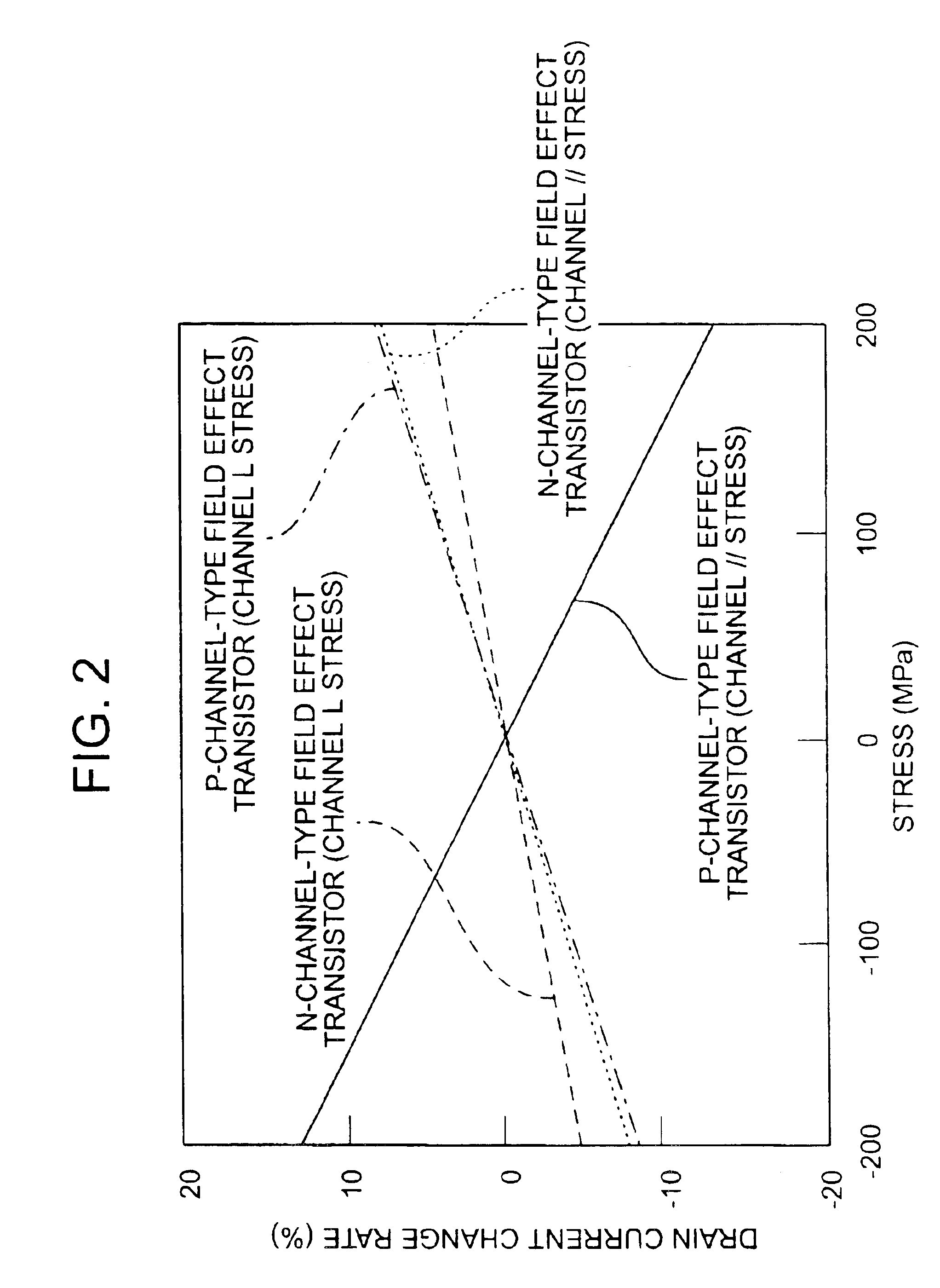
[0143]FIG. 1 is a typical sectional view of a semiconductor device according to the first embodiment of the present invention. FIG. 2 shows a stress dependence of a drain current of n- and p-channel-type field effect transistors. FIG. 3 shows a result of analyzing a stress of an effect of an intrinsic stress of an SiN film covering a gate electrode from an upper surface on a channel partial stress (the channel face stress parallel to the drain current). FIG. 8 shows an etching rate dependence of the SiN film stress. FIG. 31 shows an example of providing a wiring, etc. for the semiconductor device shown in FIG. 1.
[0144]The semiconductor device according to the first embodiment of the present invention comprises, as shown in FIG. 1, an n-channel-type field effect transistor 10 formed on a main surface of a silicon substrate 1, a p-channel-type field effect transistor 30, stress control insulate...
third embodiment
[0171]Described below will be the effect of the operation of the semiconductor device according to the
[0172]FIG. 4 is a graph of the analysis result of the film thickness dependence of the stress control film covering the gate electrode. In FIG. 4, if the stress control film indicates tensile stress, and the film thickness is large, then the stress of the channel portion is shifted to the tensile stress side. On the other hand, if the stress control film indicates compression stress, and the film thickness is large, the stress of the channel is shifted to the compression stress side.
[0173]According to the first embodiment of the present invention, if the stress control film indicates tensile stress, the p-channel type is thinner, and the drain current of the p-channel-type field effect transistor can be improved as shown in FIG. 9.
[0174]On the other hand, if the stress control film indicates compression stress, the drain current of the n-channel-type field effect transistor can be i...
second embodiment
[0183]Described below will be the effect of the operation of the semiconductor device according to the
[0184]According to the second embodiment, the stress of the channel portion of a field effect transistor is controlled by the areas of the stress control films 193 and 393. If the stress control film extending toward the source / drain area indicates tensile stress, then strong tensile stress can be applied to the channel portion by enlarging the area in the n-channel type, and the stress of the channel portion can be reduced by reducing the area in the p-channel type as small as possible. On the other hand, if the stress control film indicates compression stress, the opposite processes are performed.
[0185]It is further preferable that, with respect to a direction perpendicular to a drain current in these transistors, the area is set large, tensile stress is applied to the channel of the field effect transistors, and the stress of the channel portion is reduced by setting the area sma...
PUM
 Abstract
Description
Claims
Application Information