Integrated circuit

a technology of integrated circuits and circuits, applied in the field of integrated circuits, can solve the problems of deteriorating device properties, increasing chip size and cost, and foregoing methods, and achieve the effect of reducing electromagnetic coupling noise and coupling nois

Inactive Publication Date: 2006-01-03
SHARP KK
View PDF2 Cites 34 Cited by
  • Summary
  • Abstract
  • Description
  • Claims
  • Application Information

AI Technical Summary

Benefits of technology

[0020]An object of the present invention is therefore to provide an integrated circuit that is compatible with a standard IC process, and that can decrease electromagnetic coupling noises and coupling noises caused via the substrate.

Problems solved by technology

As shown in FIG. 11, device properties are deteriorated by interactions between circuit blocks, especially by digital switching noises coupled with analog circuits and RF circuits via a silicon substrate.
However, in case the RF circuits are integrated within a single chip, interference between RF circuit blocks (electric coupling via the substrate and magnetic coupling over the substrate) needs to be considered.
However, the foregoing methods have the following problems.
If a large space is created between interfering devices, a chip size and costs are increased.
Moreover, this technology is effective in an RF frequency band (coupling reduction via the substrate), but is not effective in reducing electromagnetic coupling (magnetic coupling over the substrate).
The technology of the non-patent publication 2 is not compatible with a normal CMOS process, and is therefore expensive.
Therefore, although metal wires are shielded by the technologies of the patent publications 1 and 2, pick-up noises and coupling noises that are transmitted from the silicon substrate or via the silicon substrate cannot be suppressed.
Furthermore, none of the foregoing technologies deal with interactions with active transistors that are such as to amplify the coupling.
The deep N−well technology has an effect of decreasing a value of the S21 by approximately 5 dB, but is still insufficient for a severe applied device such as an RF LNA.

Method used


Image

  • Integrated circuit
  • Integrated circuit
  • Integrated circuit

Examples


Embodiment Construction

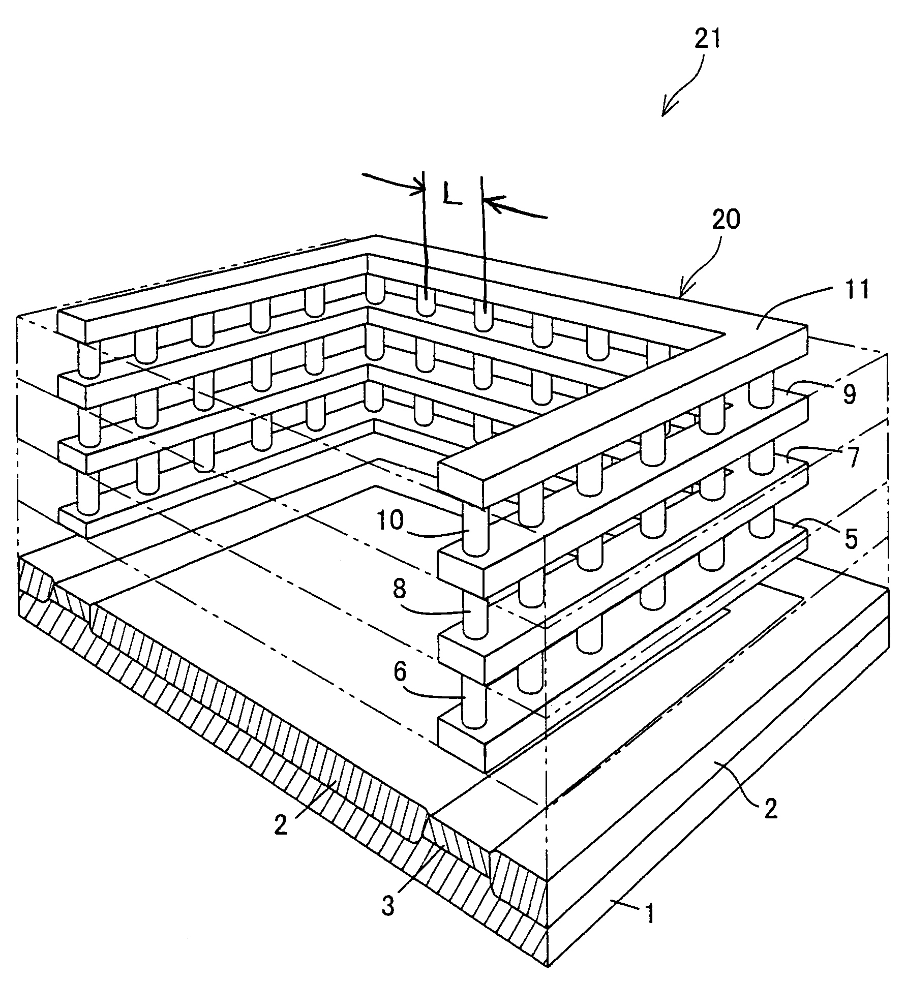
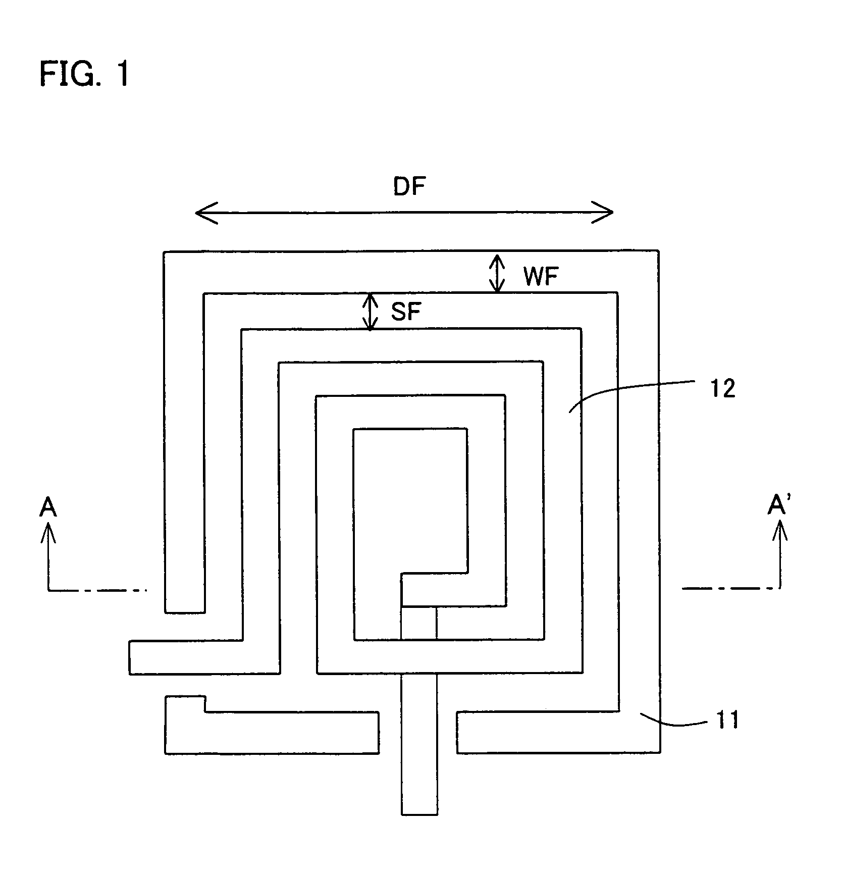
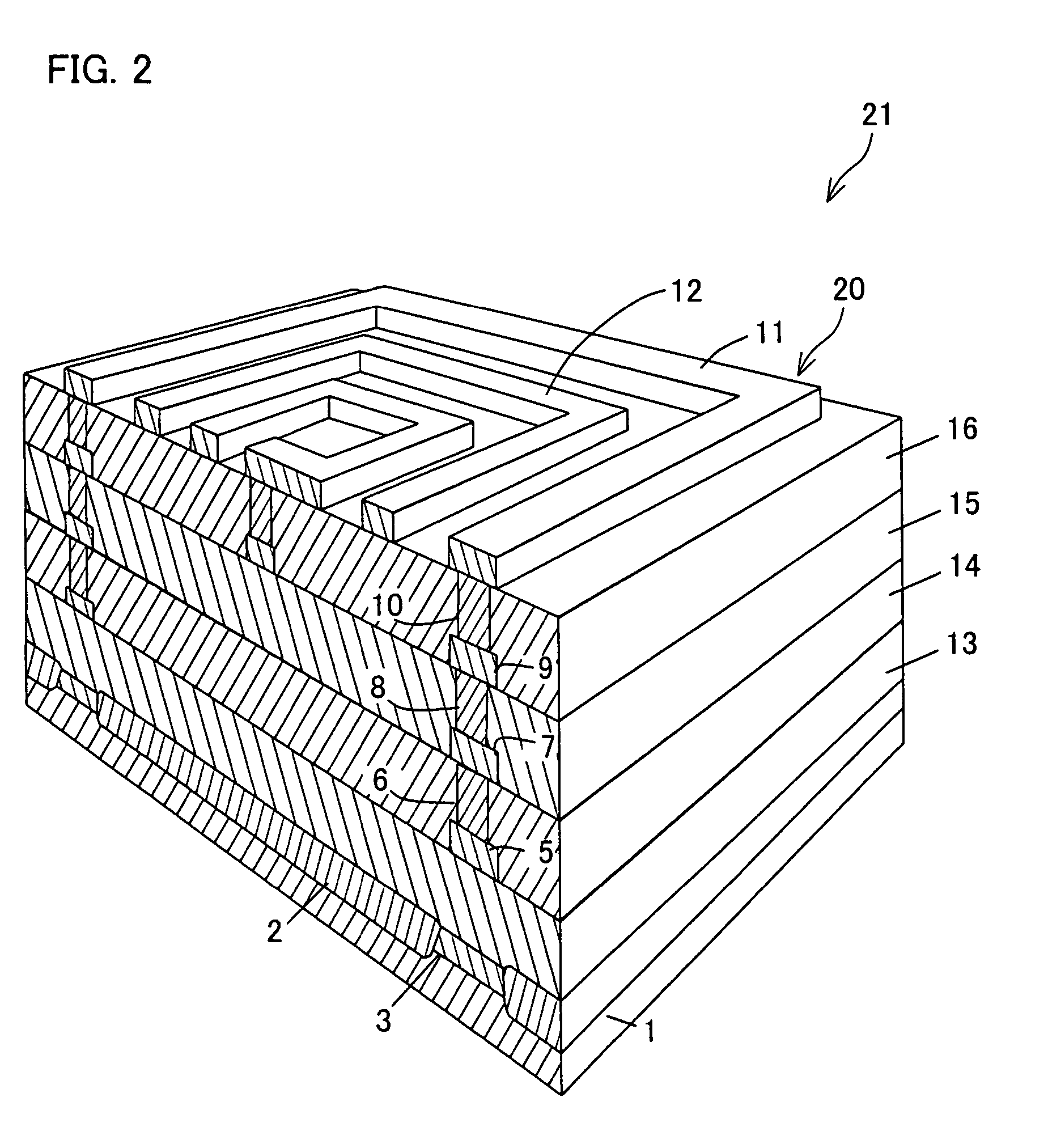
[0054]With reference to FIGS. 1 to 10, the following describes one embodiment of the present invention.

[0055]The present invention relates to electromagnetic isolation of a circuit block in an integrated circuit. In particular, the present invention proposes an electromagnetic isolation structure that is more effective for decreasing electromagnetic coupling in an RF frequency domain. The structure is effective for a standard CMOS, BiCMOS, or bipolar process. All the following structures can prevent the electromagnetic coupling in the high-frequency domain and substrate crosstalk. Here, each circuit block is a high-frequency device that is an element (a target element) generating an electromagnetic field in the integrated circuit. For example, the circuit block is a passive member such as a spiral inductor.

[0056]In an arrangement of the present embodiment, electromagnetic coupling between circuit blocks and between (i) a circuit block and (ii) interconnecting wires are prevented by ...


PUM


Abstract

A lamination of metal wire layers forms an electromagnetic isolation structure. The metal wire layers are connected with each other by vias, so that a metal fence having a laminated structure is formed. The metal fence is provided so as to surround an element (e.g. a spiral inductor) that generates an electromagnetic field in an integrated circuit. The metal wire satisfies d≦λ/8, WF≧5δ, and L≦λ/20, where δ is a skin depth of an electromagnetic wave, c is a velocity of light, f is an operating frequency of the integrated circuit, d is a lateral-direction size of a metal-fence region, WF is a surrounding-line width of the metal fence, L is an interval between the vias, and λ=c/f is a wavelength of a signal. With this arrangement, it is possible to decrease electromagnetic coupling noises and coupling noises caused via the substrate.

Description

[0001]This nonprovisional application claims priority under 35 U.S.C. § 119(a) on Patent Application No. 2003 / 102118 filed in Japan on Apr. 4, 2003, the entire contents of which are hereby incorporated by reference.FIELD OF THE INVENTION[0002]The present invention relates to an integrated circuit, and especially relates to an integrated circuit that requires consideration of electromagnetic coupling in an RF frequency domain.BACKGROUND OF THE INVENTION[0003]A system-on chip (SOC) is an integrated circuit including, within a single chip, a plurality of circuits for digital signals, analog signals, and high-frequency waves. As shown in FIG. 11, device properties are deteriorated by interactions between circuit blocks, especially by digital switching noises coupled with analog circuits and RF circuits via a silicon substrate. In a field of CMOS-hybrid-device design, it is a well-known measure to use a deep N−well in order to decrease coupling of the digital switching noises via the sub...

Claims


Application Information

Patent Timeline
Patent Type & Authority Patents(United States)
IPC IPC(8): H01L29/72H01L23/52H01L21/3205H01L21/822H01L23/522H01L23/552H01L23/58H01L27/04
CPCH01L23/552H01L23/585H01L23/645H01L23/66H01L23/5227H01L2924/0002H01L2924/3011H01L2924/00A61G7/0005A61G7/02A61G7/05
Inventor ADAN, ALBERTO O.
Owner SHARP KK
Why Eureka
Try Eureka