

Reduced area imaging devices utilizing selected charge integration periods
- Summary
- Abstract
- Description
- Claims
- Application Information
AI Technical Summary
Benefits of technology
Problems solved by technology
Method used
Image

Examples
second embodiment
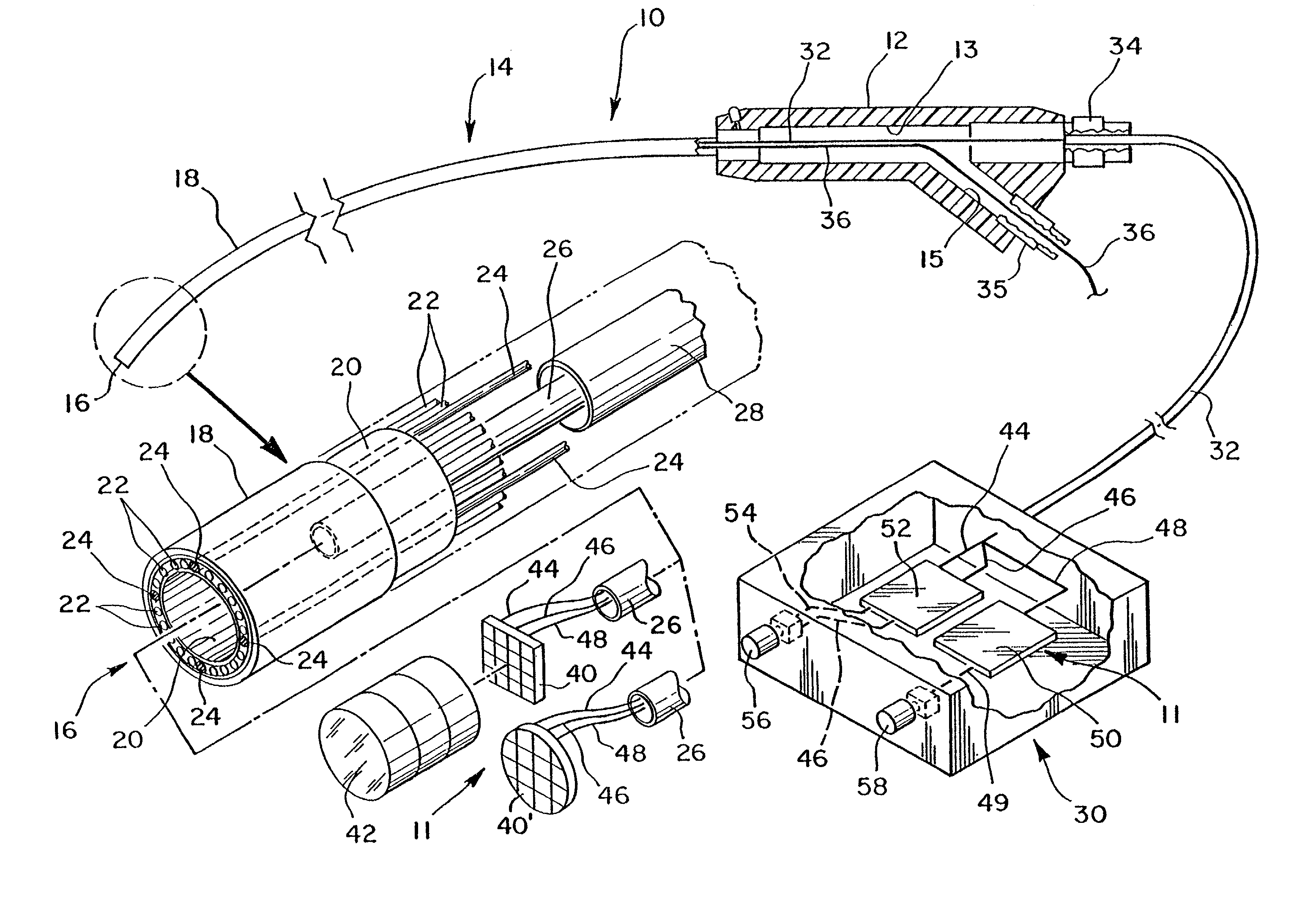
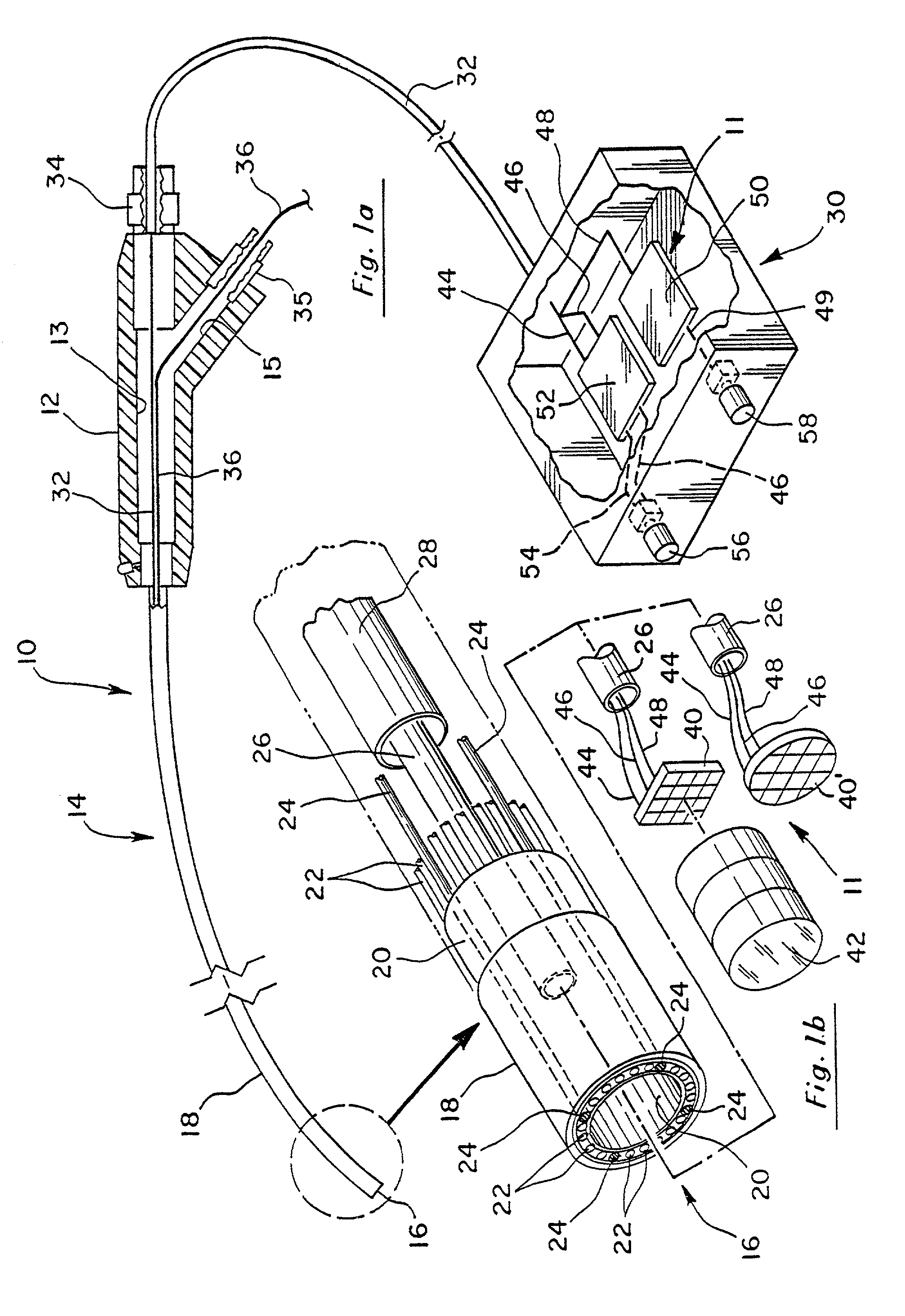
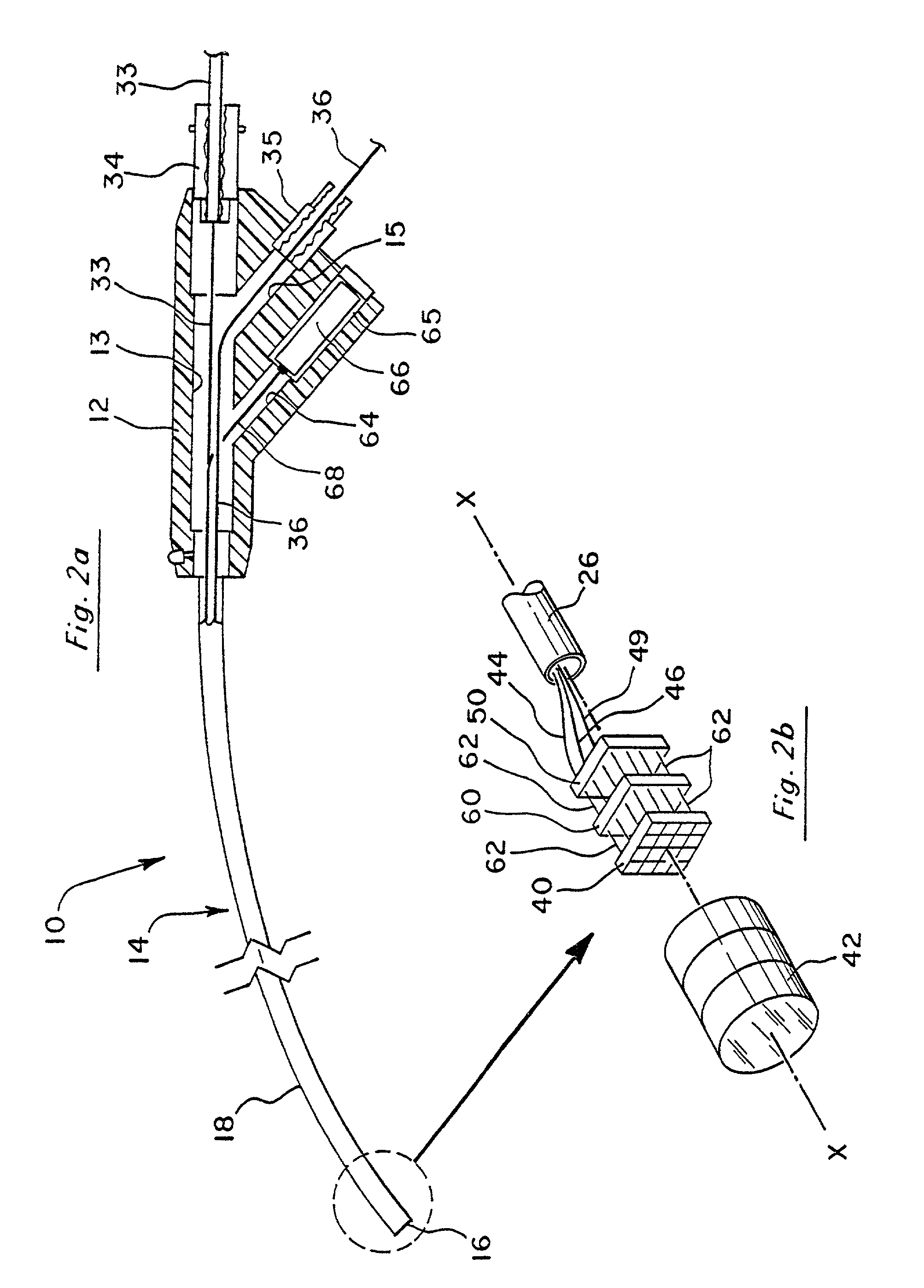
[0054]FIG. 2a illustrates this invention wherein the imaging device is self-contained entirely within the distal end 16 of the endoscope, and a power source which drives the circuitry within the imaging device may come from a battery 66 housed within handle portion 12.
[0055]As shown in FIG. 2b, the video processing board 50 may be placed directly behind image sensor 40. A plurality of pin connectors 62 serve to electrically couple image sensor 40 with video processing board 50 depending upon the specific configuration of image sensor 40, pin connectors 62 may be provided either for structural support only, or to provide a means by which image signals are transmitted between image sensor 40 and board 50. When necessary, one or more supplementary boards 60 may be provided which further contain processing circuitry to process the image signal and present it in a form which may be directly received by a desired video device. The area which is occupied by image sensor 40 may be defined a...
first embodiment
[0060]In the first embodiment illustrated in FIG. 1a, cable 32 can be used to house conductors 44, 46 and 48. In the embodiment shown in FIG. 2a, cable 33 can be used to house conductor 49 by itself when a battery power source is used, or alternatively, cable 33 may house conductors 44, 46 and 49 if the embodiment of FIG. 2a utilizes a power source from board 52.
[0061]Optionally, a supplementary processing board 60 may be provided to further enhance the pre-video signal. As shown in FIG. 4, the supplementary board 60 may be placed such that the pre-video signal from image sensor 40 is first sent to the supplementary board and then output to the video processor board 50. In this case, the output from board 50 can be carried along conductor 51. This output can be defined as an enhanced pre-video signal. Furthermore, the post-video signal from video processor board 50 may return to the supplementary board 60 for further processing, as further discussed below. The conductor used to tran...
PUM
 Abstract
Description
Claims
Application Information