Low phase noise MOS LC oscillator

a mos and low phase noise technology, applied in the direction of oscillator, pulse automatic control, pulse technique, etc., can solve the problems of lc oscillators of the prior art that fall far short of the minimum performance requirements of many today's wireless communication systems, the effect of 1/f noise characteristics, and the final phase noise is higher, so as to reduce the gain of frequency dependent amplifiers and reduce phase nois

Inactive Publication Date: 2006-01-17
MARVELL INT LTD
View PDF7 Cites 40 Cited by
  • Summary
  • Abstract
  • Description
  • Claims
  • Application Information

AI Technical Summary

Benefits of technology

[0039]To accomplish these and other objects, an oscillator having low phase noise that is formed of a frequency dependent amplifier to amplify a signal having a fundamental frequency; a frequency dependent feedback device that is connected between an output of the frequency dependent amplifier and an input of the frequency dependent amplifier to feed a portion of an amplifi...

Problems solved by technology

LC oscillators of the prior art fall far short of the minimum performance requirements of many of today's wireless communication systems.
These shifts are caused by thermal noise, shot noise, and flicker noise (1/f noise).
Unfort...

Method used


Image

  • Low phase noise MOS LC oscillator
  • Low phase noise MOS LC oscillator
  • Low phase noise MOS LC oscillator

Examples


second embodiment

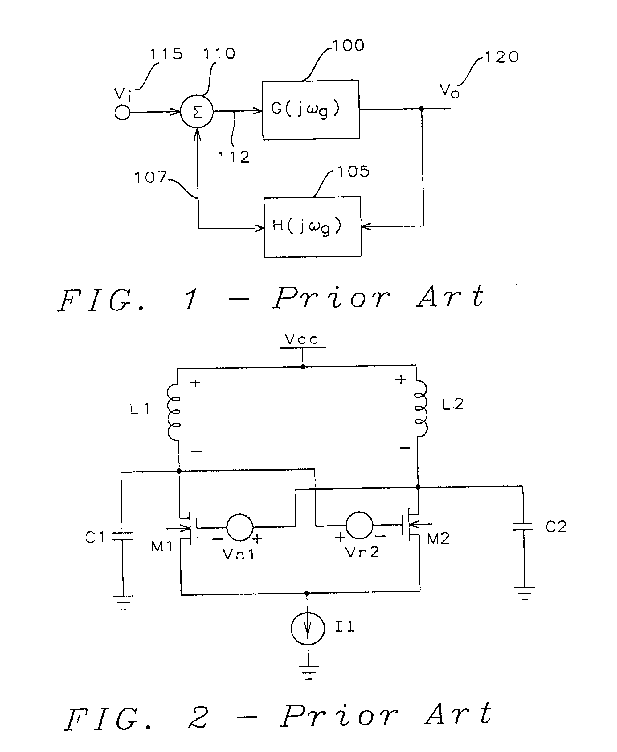
[0080]FIG. 5b illustrates a cross-coupled differential NMOS oscillator of this invention. The frequency dependent gain amplifier in this case is formed by the NMOS transistors M1 and M2 and the resistors R1 and R2. The resistor R1 is connected between the source of the NMOS transistor M1 and the ground reference point. The resistor R2 is connected between the source of the NMOS transistor M2 and the ground reference point.

[0081]The inductor L1 is connected from the drain of the NMOS transistor M1 to the reference voltage source Vcc and the inductor L2 is connected from the drain of the NMOS transistor M2 to the reference voltage source Vcc. The capacitor C1 is connected from the drain of NMOS transistor M1 to the ground reference point and the capacitor C2 is connected from the drain of the NMOS transistor M2 to the ground reference point. As described above, it is apparent to those skilled in the art that, while the capacitors C1 and C2 are connected to the ground reference point, ...

third embodiment

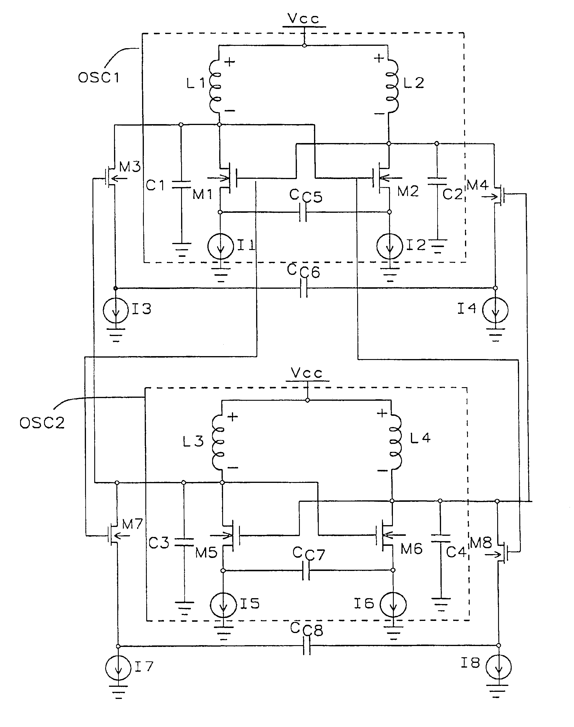
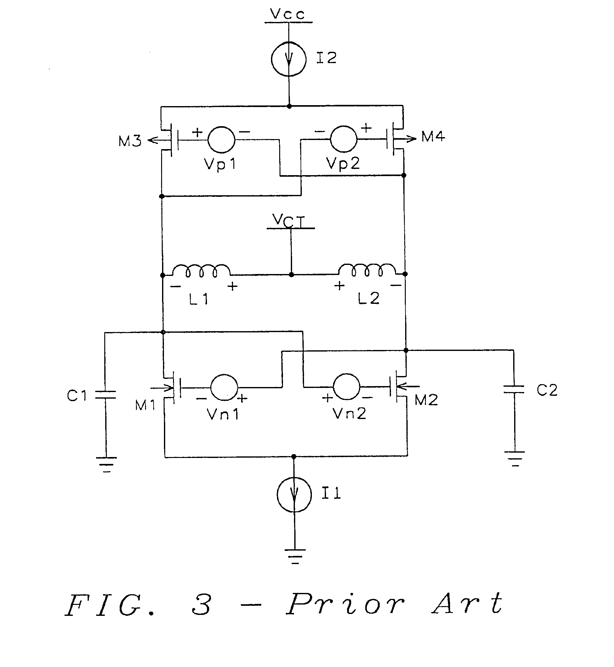
[0083]this invention, as shown in FIG. 7, implements the frequency dependent gain circuit as a cross-coupled differential CMOS amplifier. The frequency dependent gain circuit is formed by the NMOS transistors M1 and M2, the P-type MOS (PMOS) transistors M3 and M4, and the current sources I1, I2, I3, and I4.

[0084]The drain of the NMOS transistor M1 is connected to the gate of the NMOS transistor M2 and the drain of the NMOS transistor M2 is connected to the gate of the NMOS transistor M1. Similarly, the drain of the PMOS transistor M3 is connected to the gate of the PMOS transistor M4 and the drain of the PMOS transistor M4 is connected to the gate of the PMOS transistor M3. The cross-coupling of the drains and gates of the NMOS transistors M1 and M2 and the PMOS transistors M3 and M4 forms the feedback circuit of the oscillator.

[0085]The inductor L1 is connected between the drains of the NMOS and PMOS transistors M1 and M3 and the reference voltage source VCT. The inductor L2 is con...


PUM


Abstract

A cross-coupled differential MOS oscillator having reduced phase noise is applicable to a RF communication device such as a transmitter or receiver. The oscillator having low phase noise is formed of a frequency dependent amplifier to amplify a signal having a fundamental frequency; a frequency dependent feedback device that is connected between an output of the frequency dependent amplifier and an input of the frequency dependent amplifier to feed a portion of an amplified signal having the fundamental frequency to an input of the frequency dependent amplifier to stimulate oscillation; and a attenuating device in communication with the frequency dependent amplifier. The attenuating device reduces the gain of the frequency dependent amplifier for signals having frequencies much, much less than the fundamental frequency to decrease the phase noise.

Description

[0001]This application is a continuation of, and hereby claims priority under 35 U.S.C. §120 on, U.S. application Ser. No. 09 / 699,772 filed on Sep. 26, 2000, now U.S. Pat. No. 6,376,101 the entire contents of which are hereby incorporated herein by reference, which is based on, and which claims priority under 35 U.S.C. §120 on, provisional patent application, 60 / 204,885, filed on May 17, 2000.BACKGROUND OF THE INVENTION[0002]1. Field of the Invention[0003]This invention relates to high frequency oscillator circuits. More particularly, this invention relates to metal oxide semiconductor (MOS) oscillators having low phase noise.[0004]2. Description of the Related Art[0005]Inductive / capacitive (LC) oscillators are important elements of any Radio Frequency (RF) communication devices, such as transmitters, where the LC oscillators are used as master oscillators, or as receivers where the LC oscillators are used as local oscillators. An important performance benchmark of an LC oscillator ...

Claims


Application Information

Patent Timeline
IPC IPC(8): H03L5/00
CPCH03B1/04H03B27/00H03B5/1215H03B5/1228H03B2200/0078
Inventor SUTARDJA, SEHAT
Owner MARVELL INT LTD
Why Eureka
Try Eureka