Forming an optical element on the surface of a light emitting device for improved light extraction

a technology of light-emitting devices and optical elements, which is applied in the direction of optics, semiconductor devices, instruments, etc., can solve the problems of low light extraction efficiency, achieve the effects of improving light extraction, easy integration, and maximizing production efficiency

Inactive Publication Date: 2006-01-17
LUMILEDS
View PDF54 Cites 202 Cited by
  • Summary
  • Abstract
  • Description
  • Claims
  • Application Information

AI Technical Summary

Benefits of technology

[0012]Stamping is an alternative way of forming an optical element on the surface of a light emitting device. The stamping process is carried out at a temperature above the ductile transition point of the semiconductor material that is to be stamped. In one embodiment, stamping is integrated with wafer-bonding process. As a wafer-bonding process is commonly executed in an environment with temperature in the vicinity of 600° C. or higher, the stamping process can be readily integrated with the wafer-bonding process to maximize production efficiency. A wafer-bonding process entails removing the original absorptive substrate that was used as a template to grow epitaxial layers of the desired quality and replacing it with a transparent substrate to improve light extraction. Optionally, at the time the transparent substrate is bonded to a first surface of semiconductor light emitter 100, a stamping block with a shape or a pattern that is the inverse of the shape or the pattern of the desired optical element can be pressed against a second surface of semiconductor light emitter 100, a surface of the transparent substrate, or both surfaces. When the pressure is released, a light emitting device having a surface that is shaped into the desired optical element is formed. The stamping block used for stamping usually has a higher melting point temperature than the process temperature that is applied during the formation of the optical element. Suitable materials for stamping block include but are not limited to molybdenum alloys, graphite, silicon carbide, and sapphire. The optical element may be formed on one or more surfaces of semiconductor light emitter. Although the stamping process is an independent process, it may optionally be used before, after, or concurrently with the wafer-bonding process. Alternatively, it may be used to stamp a material that is later bonded to semiconductor light emitter 100.
[0014]The effectiveness of the present invention can be enhanced by increasing the proportion of the photons that are emitted toward a preselected portion of the optical element. For example, a confined-emission spot LED may be made to emit an increased proportion of the emitted photons toward the center of a Fresnel lens because the photons that reach the edge of a Fresnel lens benefit less from the presence of the Fresnel lens. Methods that can confine photon emission to selected areas of the active layer include ion implantation, diffusion, oxide passivation, selective area growth, and selective area bonding. Alternatively, the outer edges of semiconductor light emitter 100 or active layer 22 may be etched away. Etching away the outer edges may produce a light emitting device with beveled sides.

Problems solved by technology

A problem with LEDs is a low light extraction efficiency.

Method used


Image

  • Forming an optical element on the surface of a light emitting device for improved light extraction
  • Forming an optical element on the surface of a light emitting device for improved light extraction
  • Forming an optical element on the surface of a light emitting device for improved light extraction

Examples


Embodiment Construction

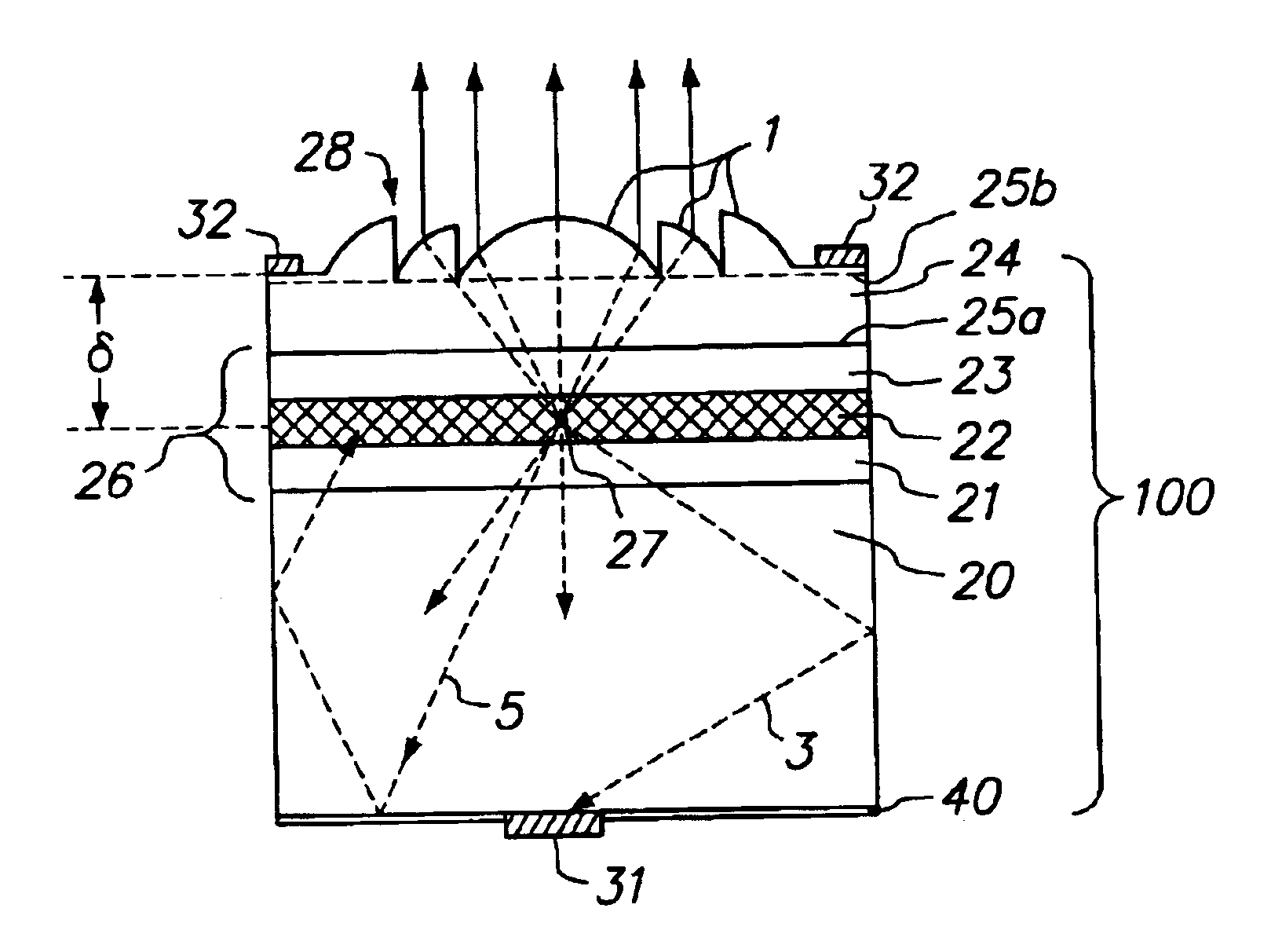
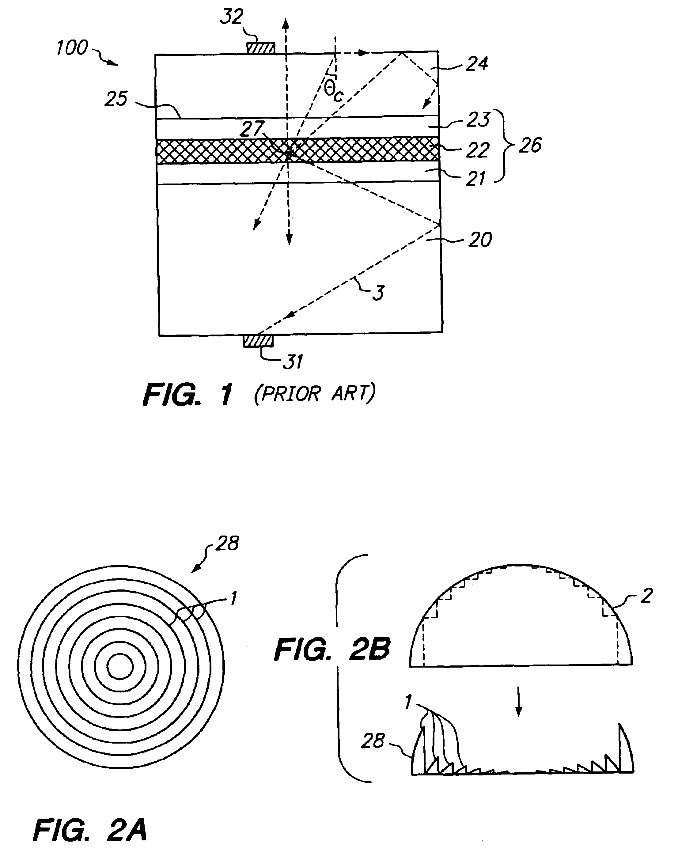
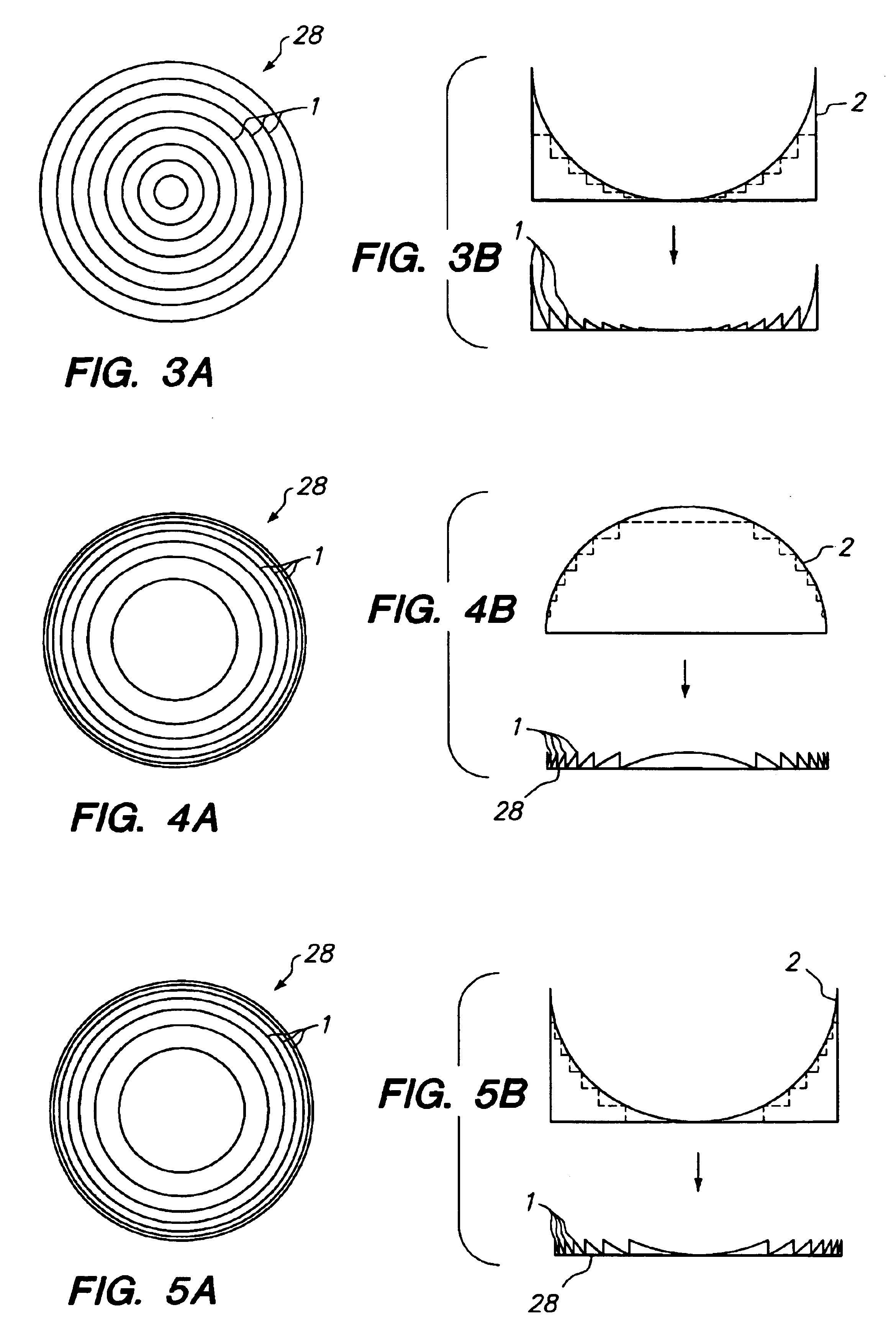
[0042]As used herein, the “extraction surface” refers to the surface of a light emitting device intended to be the light output surface. A light emitting device may have more than one extraction surface. For convenience of illustration, the figures show the extraction surface as the top surface. The light emitting device may be an LED. The light generating portions of the LEDs described herein may be conventional active layers of an LED. A “light emitting device,” as used herein, includes a device including at least one semiconductor light emitter 100. The present invention includes both stamping the surface of a light emitting device into an optical element and forming a Fresnel lens or a holographic diffuser on the surface of a light emitting device using any method including stamping. Although the present invention also includes a holographic diffuser formed on the surface of a light emitting device, the examples and descriptions refer mainly to Fresnel lens for clarity of illust...


PUM


Abstract

Provided is a light emitting device including a Fresnel lens and / or a holographic diffuser formed on a surface of a semiconductor light emitter for improved light extraction, and a method for forming such light emitting device. Also provided is a light emitting device including an optical element stamped on a surface for improved light extraction and the stamping method used to form such device. An optical element formed on the surface of a semiconductor light emitter reduces reflective loss and loss due to total internal reflection, thereby improving light extraction efficiency. A Fresnel lens or a holographic diffuser may be formed on a surface by wet chemical etching or dry etching techniques, such as plasma etching, reactive ion etching, and chemically-assisted ion beam etching, optionally in conjunction with a lithographic technique. In addition, a Fresnel lens or a holographic diffuser may be milled, scribed, or ablated into the surface. Stamping, an alternative method for forming an optical element, can also be used to form a Fresnel lens or a holographic diffuser on the surface of a semiconductor light emitter. Stamping includes pressing a stamping block against the surface of a light emitting diode. The stamping block has a shape and pattern that are the inverse of the desired optical element. Optionally, stamping can be done before, after, or concurrently with wafer-bonding. Alternatively, a material can be stamped and later bonded to the semiconductor light emitter.

Description

BACKGROUND[0001]1. Technical Field[0002]The invention relates generally to light-emitting devices and more particularly to light emitting devices with improved light extraction.[0003]2. Description of the Prior Art[0004]FIG. 1 depicts a prior art semiconductor light emitter 100 consisting of substrate 20, multi-layered structure 26, and top layer 24. Semiconductor light emitter 100 may be, for example, a light emitting diode (“LED”) or a semiconductor laser. An LED is a p-n junction device that is designed to convert an incoming flow of electric energy into an outgoing flow of electromagnetic radiation. An LED may emit electromagnetic radiation in ultraviolet, visible, or infrared regions of the electromagnetic spectrum. The visible LEDs are commonly used for illumination and displays, and also have applications as an information link between electronic instruments and their users. The infrared LEDs are useful in opto-isolators and optical-fiber communications. A semiconductor laser...

Claims


Application Information

Patent Timeline
Patent Type & Authority Patents(United States)
IPC IPC(8): G02B27/44G02B5/18G02B5/32H01L33/20H01L33/44
CPCG02B5/32H01L33/20H01L33/44
Inventor POCIUS, DOUGLAS W.CAMRAS, MICHAEL D.HOFLER, GLORIA E.
Owner LUMILEDS
Why Eureka
Try Eureka