Copper foil for printed-wiring board and copper-clad laminate using copper foil for printed-wiring board

a technology of copper foil and printed wire, which is applied in the field of copper foil for printed wire and copper foil for copperclad laminate, can solve the problems of increasing generation, difficult processing, and no means for purposely improving chemical resistance and heat resistance, and achieve excellent ul heat resistance

Inactive Publication Date: 2006-01-24
MITSUI MINING & SMELTING CO LTD
View PDF19 Cites 20 Cited by
  • Summary
  • Abstract
  • Description
  • Claims
  • Application Information

AI Technical Summary

Benefits of technology

[0023]The specific surface area of the nodular treatment side of a general copper foil varies depending on the thickness of the copper foil. Therefore, if the thickness of the nickel-zinc alloy layer is smaller than 0.7 g per square meter of nodular treatment side of the copper foil, stability is reduced in the sense that the nodular treatment side of the normally conceivable whole thickness of copper foil is covered uniformly and without irregularity. If the thickness of the nickel-zinc alloy layer exceeds 45 g per square meter, the irregularities for obtaining the anchor effect of the nodular treatment side of the normally conceivable whole thickness of copper foil may be eliminated or changed into a flat shape. Thus, the thickness derived as optimum conditions allowing the nickel-zinc alloy layer to be formed as a surface treatment layer for the nodular treatment side of the normally conceivable whole thickness of copper foil is 0.7 g to 45 g per square meter of nodular treatment side of the copper foil.
[0028]Nickel conducts heat at a rate about ⅕ of the heat conductivity of copper. Also, because of its high absorptance for laser beams, nickel has a high efficiency of conversion to heat energy compared to copper. Therefore, it can be considered that heat energy is easily concentrated on the site exposed to the laser beam, and the speed at which heat energy is supplied by the laser beam than the speed at which heat is diffused, and the site exposed to the laser beam easily reaches the melting point of nickel, thus improving laser drilling processability. If the aforementioned absorptance for laser beams is compared for copper and nickel having same levels of surface roughness, the reflectivity of nickel is apparently smaller than that of copper by about 1% to 2%, and thus the absorptance for laser beams by nickel is higher.
[0030]Here, what is brought about as another effect is that a solution capable of dissolving the resin of the insulation resin layer is used for the solution of desmear treatment, and therefore it vanishes even irregularities on the outer face of the substrate, thus reducing the adhesion to the substrate of a copper layer subsequently formed by the plating method or the like. If using copper foil for printed-wiring board according to present invention, however, irregularities on the outer face of the substrate remain intact so that the anchor effect can be obtained because the nickel-zinc alloy layer exists on the outermost layer, thus making it possible to improve adhesion between the plated layer and the substrate.
[0031]From this point, a copper plated layer is formed on the entire surface of the substrate including the inner wall of the via hole 14 in the case of the plating method, as shown in FIG. 4D. Then, as shown in FIG. 4E, an etching resist layer 16 is formed on the surface of the copper plated layer 15, and as shown in FIG. 5F, a circuit pattern is developed by light exposure on the etching resist layer 16, and a acid etchant for copper is used to carry out circuit etching, and the etching resist is peeled off to obtain the printed-wiring board 18 as shown in FIG. 15G. If the above described production method is adopted, the nickel-zinc layer 5 exists in the interface between the circuit on the outer face and the substrate, thus making it possible to obtain a plate having excellent UL heat resistance.
[0032]When the semiadditive method is adopted, on the other hand, the following flow is applied. For the plate shown in FIG. 3C that has been subjected to laser drilling processing to form the shape of the via hole 14 and has undergone desmear treatment, the etching resist layer 16 is formed on the surface of the exposed nickel-zinc layer 5 as shown in FIG. 6D without forming a plated layer, a circuit pattern is developed by light exposure on the etching resist layer 16 as shown in FIG. 6E, the nickel-zinc layer 5 is etched into a circuit shape using an etchant, and the etching resist is peeled off to provide a situation shown in FIG. 7F. Then, the copper plated layer 15 is formed on the nickel-zinc layer 5 shaped like a circuit and on the inner wall of the via hole 14, whereby the printed-wiring board 18 as shown in FIG. 7G can be obtained. Adoption of this production method makes it possible to obtain a plate having excellent UL heat resistance in which the nickel-zinc layer 5 exists in the interface between the circuit and the substrate in a same way as FIG. 5G.
[0035]Therefore, uses similar to those of the copper foils described above can be adopted for this copper foil for printed-wiring board, and the printed-wiring board obtained by a production method similar to those described above allows a fine pitch circuit to be easily formed, and enables a circuit having UL heat resistance to be provided.

Problems solved by technology

As the wiring density of the printed-wiring board is increased and components implemented therein are further integrated, the amount of heat generation is increased, thus causing a problem.
However, for processing fine via holes and the like, laser drilling processing has been used in recent years, thus making it difficult to process the via hole with the copper foil bonded thereto, and therefore the conformal mask method in which the outer-layer copper foil is partially etched away to carry out laser drilling processing, the method in which the outer-layer copper foil for improving accuracy of position for drilling process is wholly etched away, and so on are employed.
The problem arising in such methods is that after the copper foil is once removed, a surface treatment layer that would exist if the original copper foil were used does not exist in the interface between the circuit formed by the panel plating method or the additive method and the substrate.
That is, absence of the surface treatment layer means that in the circuit portion is provided no means for purposely improving its chemical resistance and heat resistance.

Method used


Image

  • Copper foil for printed-wiring board and copper-clad laminate using copper foil for printed-wiring board
  • Copper foil for printed-wiring board and copper-clad laminate using copper foil for printed-wiring board
  • Copper foil for printed-wiring board and copper-clad laminate using copper foil for printed-wiring board

Examples


example 1

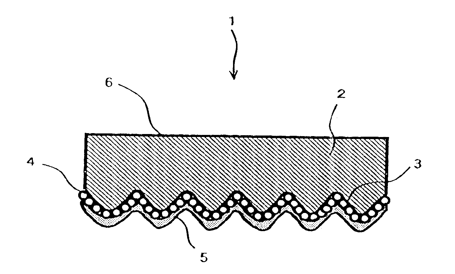
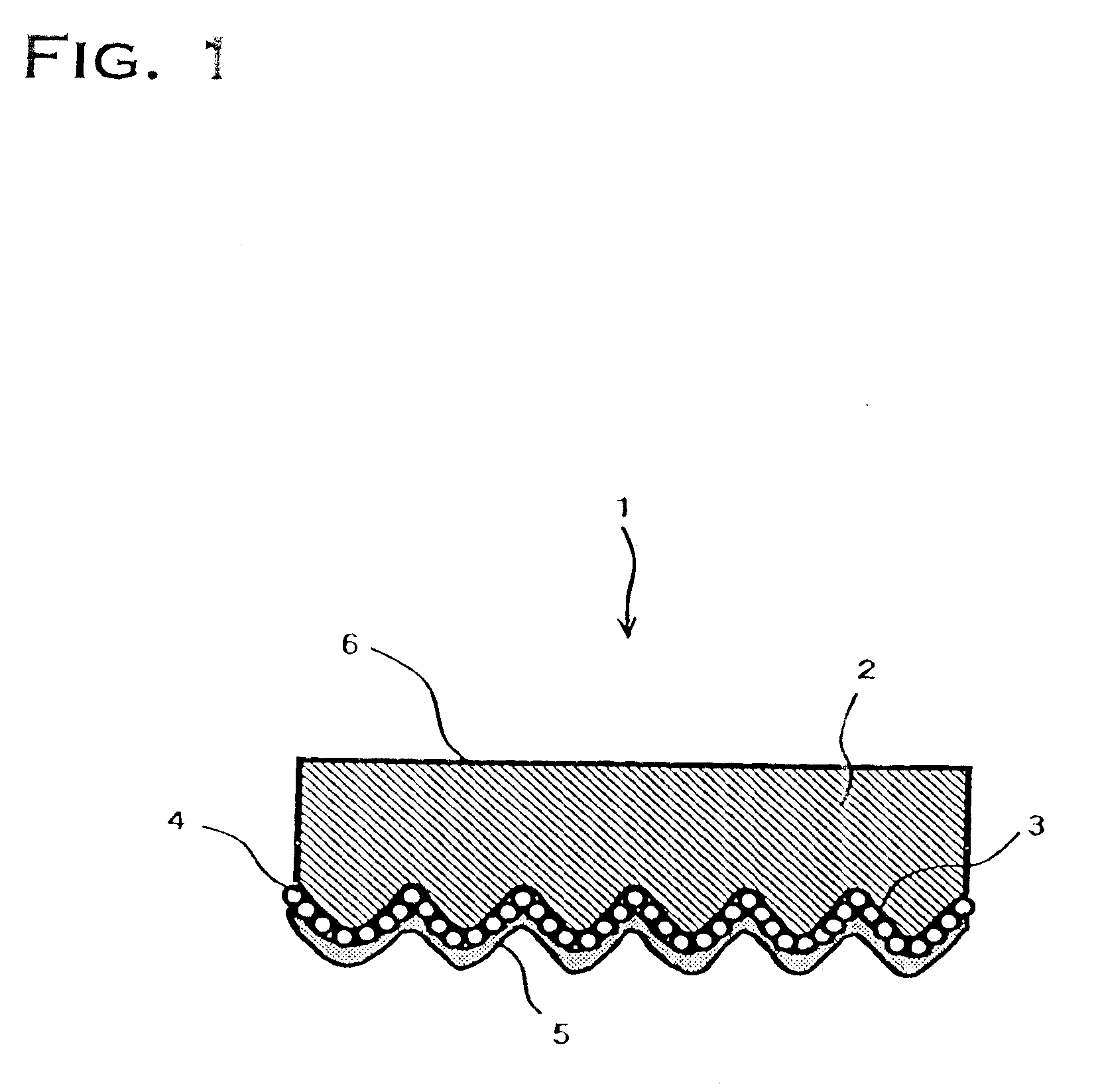
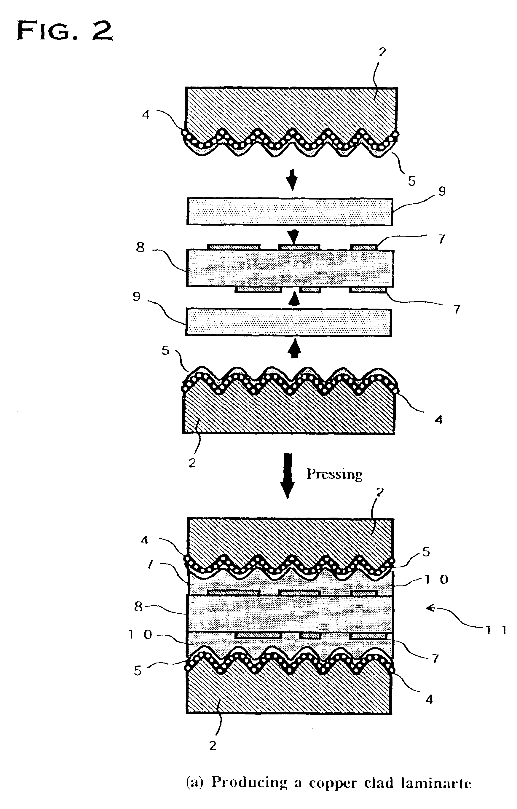
[0045]In this Example, the steps of producing a printed-wiring board using a copper foil for printed-wiring board comprising an alloy layer of nickel and zinc on the matte side of an electrodeposited copper foil will be described. First, production of the copper foil for printed-wiring board 1 will be described with reference to the drawings. Here, an electrodeposited copper foil having a cross section shown schematically in FIG. 1 for use in producing a copper foil having nominal thickness of 18 μm, which had not been subjected to surface treatment (hereinafter referred to as “untreated copper foil”) was used. Then, a so called surface treatment apparatus was used to subject this untreated copper foil 2 to nodular treatment and surface treatment for forming the nickel-zinc layer.

[0046]In the surface treatment apparatus, copper microparticles 4 are first deposited on the surface of the matte side 3 of the untreated copper foil 2 under burnt copper plating conditions. For the burnt c...

example 2

[0054]In this Example, the steps of producing a printed-wiring board with the use of a copper foil for printed-wiring board comprising an alloy layer of nickel and zinc on the matte side of an electrodeposited copper foil will be described. First, production of the copper foil for printed-wiring board 1 will be described with reference to the drawings. Here, an electrodeposited copper foil having a cross section shown schematically in FIG. 1 for use in producing a copper foil having nominal thickness of 18 μm, which had not been subjected to surface treatment (hereinafter referred to as “untreated copper foil”) was used. Then, a so called surface treatment apparatus was used to subject this untreated copper foil 2 to nodular treatment and surface treatment for forming the nickel-zinc layer.

[0055]In the surface treatment apparatus, copper microparticles 4 are first deposited on the surface of the matte side 3 of the untreated copper foil 2 under burnt copper plating conditions, and s...

example 3

[0058]In this Example, the steps of producing a printed-wiring board using a copper foil for printed-wiring board comprising two layers, namely nickel and zinc layers on the nodular treatment side of an electrodeposited copper foil will be described. First, production of the copper foil for printed-wiring board 1 will be described with reference to the drawings. Here, an electrodeposited copper foil having a cross section shown schematically in FIG. 8 for use in producing a copper foil having nominal thickness of 18 μm, which had not been subjected to surface treatment (hereinafter referred to as “untreated copper foil”) was used. Then, a so called surface treatment apparatus was used to subject this untreated copper foil 2 to nodular treatment and surface treatment for forming the nickel and zinc layers.

[0059]In the surface treatment apparatus, copper microparticles 4 are first deposited on the surface of the matte side 3 of the untreated copper foil 2 under burnt copper plating co...


PUM

PropertyMeasurementUnit
thicknessaaaaaaaaaa
widthaaaaaaaaaa
boiling pointaaaaaaaaaa

Abstract

The object is to provide a copper foil excellent in the property of selective etching between a resistor layer and a copper layer required in production of a printed-wiring board, and also excellent in UL heat resistance. For this purpose, a copper foil for printed-wiring board comprising a nodular treatment side on one side, wherein a nickel-zinc alloy layer is formed on the nodular treatment side is used for applications of printed-wiring boards. At the same time, a production method suitable for production of the copper foil is provided.

Description

CROSS-REFERENCE TO RELATED APPLICATIONS[0001]The present application is a national stage filing under 35 U.S.C. §371 of PCT / JP02 / 07601, filed on Jul. 26, 2002, designating the U.S.TECHNICAL FIELD[0002]The present invention relates to a copper foil for printed-wiring board and a method of producing the same, and a copper-clad laminate using the copper foil for printed-wiring board.BACKGROUND ART[0003]For copper foils that have been conventionally used, a various kinds of copper foils are introduced to the market, and which copper foil should be used has been determined depending on the uses of printed-wiring boards. They include, for example, copper foils comprising nickel layers for forming resistors, heat-resisting copper foils to be used for sites that are exothermically affected in a direct manner by electronic equipment, and copper foils having excellent chemical resistance that are advantageously used for formation of fine pitch circuits.[0004]In the trend in recent years towar...

Claims


Application Information

Patent Timeline
Patent Type & Authority Patents(United States)
IPC IPC(8): B32B15/20H05K3/38B32B15/08C25D7/06H05K1/09C25D3/56H05K3/00H05K3/02H05K3/46
CPCH05K3/025H05K3/384C25D3/562Y10T428/12993H05K3/4652H05K2203/0307H05K2203/0376H05K2203/0384Y10S428/935Y10T428/12514Y10T428/12438Y10T428/12792Y10T428/24917Y10T428/12569Y10T428/12472Y10T428/1291H05K3/0038H05K1/09
Inventor YAMAMOTO, TAKUYATAKAHASHI, MASARUYAMADA, MASAMICHI
Owner MITSUI MINING & SMELTING CO LTD
Why Eureka
Try Eureka