Non-resolving mask tiling method for flare reduction

a non-resolving, mask technology, applied in the field of semiconductor circuits, can solve the problems of scattering bars not providing improvement for medium or long-range pattern density or flare distortion, mask or reticle variation,

Inactive Publication Date: 2006-01-24
TAIWAN SEMICON MFG CO LTD
View PDF19 Cites 34 Cited by
  • Summary
  • Abstract
  • Description
  • Claims
  • Application Information

AI Technical Summary

Problems solved by technology

As feature dimensions used in integrated circuits have become sub-micron various problems are encountered.
A major limitation with tiling is that tiling cannot be used in close proximity to functional circuitry because of negative effects on device characteristics.
Another known lithography problem is referred to as flare which is the existence of scattered background light in a lithographic system.
However the scattering bars do not provide improvement for medium or long range pattern density or flare distortion.
Another known lithographic issue is the variation of mask or reticle feature dimensions as mask pattern density varies.
Tiling offers some improvement to this issue but tiling is limited in use due to the electrical modifications on functional devices as mentioned above.
Subresolution scattering bars do not offer significant improvement to this problem.
A problem with these solutions is that they require extremely intense computation for every feature edge as to what is the impact of flare or reticle pattern density.

Method used


Image

  • Non-resolving mask tiling method for flare reduction
  • Non-resolving mask tiling method for flare reduction
  • Non-resolving mask tiling method for flare reduction

Examples


Embodiment Construction

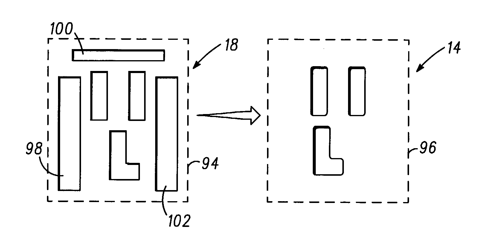
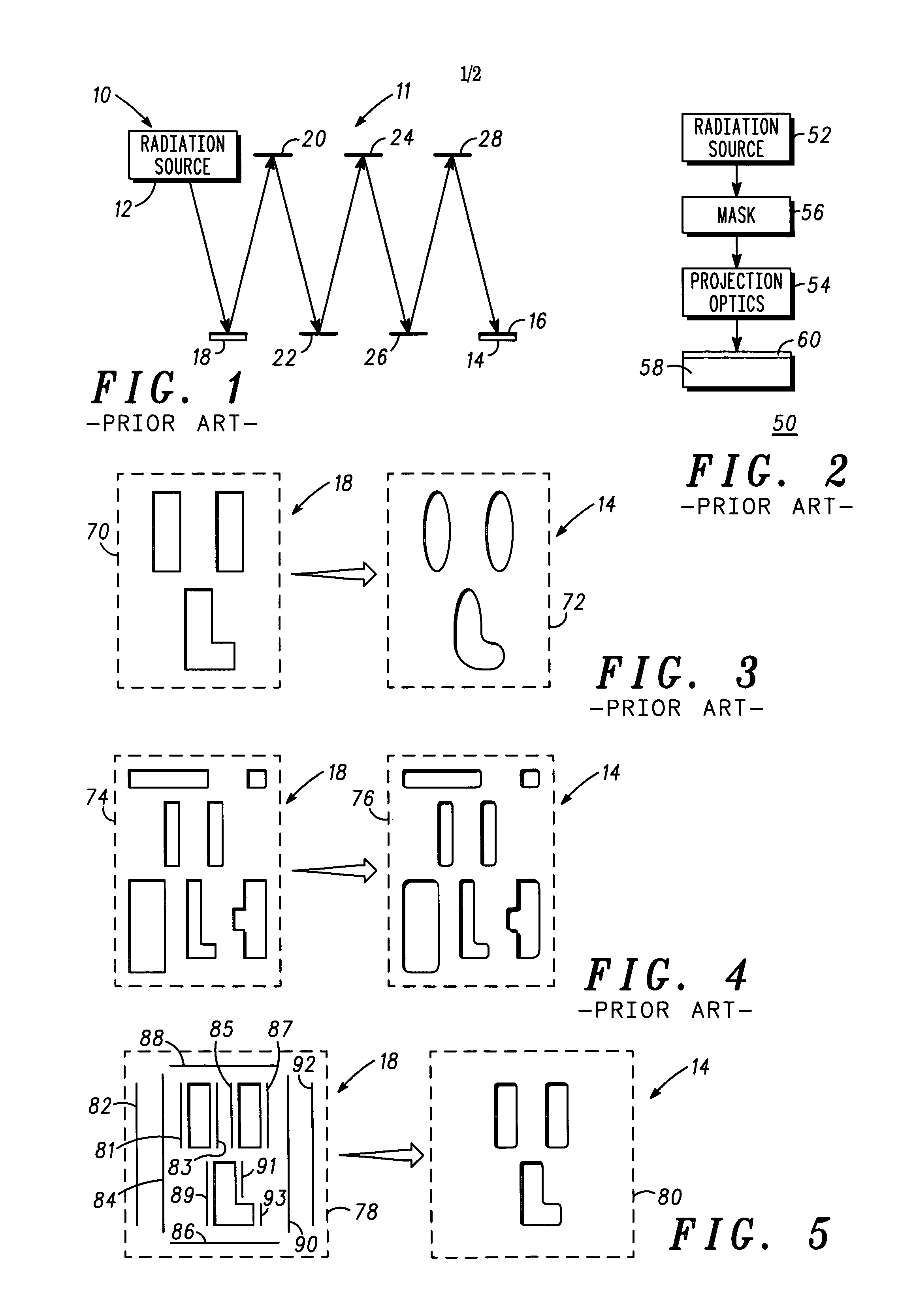
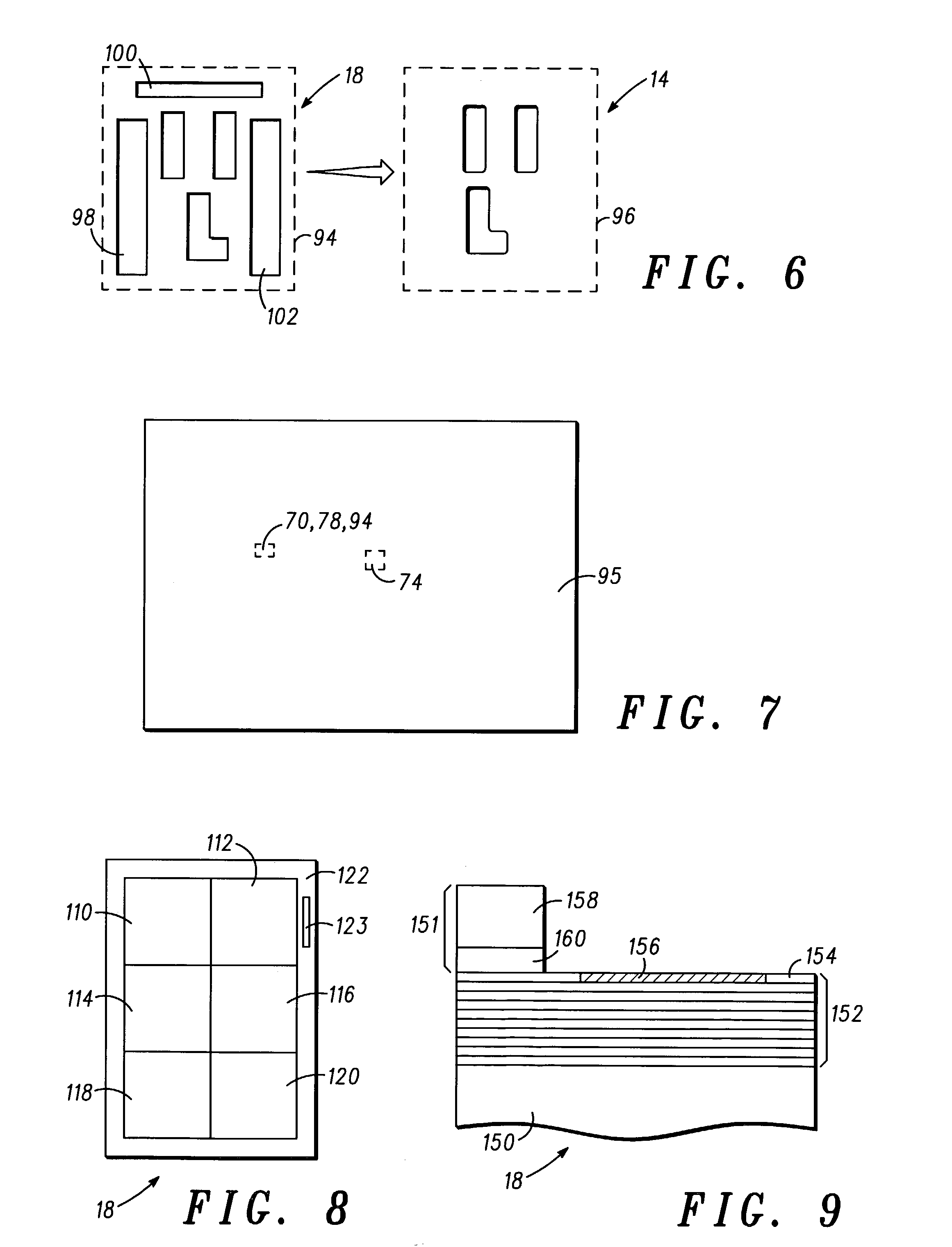
[0018]FIG. 1 illustrates an EUV lithography system or optical system 10 with an optical portion 11. Optical system 10 has a radiation source 12, a reflecting reticle or reflecting mask 18, and optical reflecting elements 20, 22, 24, 26 and 28. In one form, the optical reflecting elements 20, 22, 24, 26 and 28 are implemented with multiple layer mirrors. The radiation source 12 may be implemented in various forms such as a laser, a laser produced plasma, a gas discharge source or an electron beam source. In the illustrated form, light produced by the radiation source 12 is transferred from the radiation source 12 to the reflecting mask 18. A predetermined pattern exists on the reflecting mask 18. Portions of the predetermined pattern cause the radiation or light to reflect via the reflective mask by reflecting from reflecting mask 18 to an optical reflecting element 20. In sequential fashion the light is further reflected to optical reflecting elements 22, 24, 26 and 28. From optical...


PUM

PropertyMeasurementUnit
wavelengthaaaaaaaaaa
lengthaaaaaaaaaa
widthaaaaaaaaaa

Abstract

Photoresist on a wafer is exposed using tiles on a mask that improve flare performance. Features that are not to be exposed on the photoresist correspond to features on the mask. The various features are surrounded by other features that vary and thus affect flare differently. Selected features have tiles added nearby but also far enough away to improve uniformity in the effects of flare on the various features that are intended to be present in the photoresist. The tiles are made either very small in width or partially absorbing so that the tiles are not resolved in the photoresist. Thus the tiles reduce flare but do not alter the desired pattern in the photoresist.

Description

CROSS REFERENCE TO RELATED APPLICATION[0001]This application is related to:[0002]U.S. patent application Ser. No. 09 / 873,810, entitled “Method of Forming An Integrated Circuit Device Using Dummy Features and Structure Thereof,” filed Jun. 4, 2001, and assigned to the assignee hereof.FIELD OF THE INVENTION[0003]This invention relates generally to semiconductor circuits, and more specifically, to the manufacture of semiconductors.BACKGROUND OF THE INVENTION[0004]Integrated circuit manufacturing uses photolithography to transfer patterns from a master mask to a semiconductor substrate. As feature dimensions used in integrated circuits have become sub-micron various problems are encountered. The small dimensions approach the physical capability of photolithography. At such dimensions, the nonplanarity of surfaces, such as wafers have a significant affect on feature resolution on the wafer. A known compensation technique is the use of tiles which are additional features formed on the sem...

Claims


Application Information

Patent Timeline
Patent Type & Authority Patents(United States)
IPC IPC(8): G03F7/20C03C25/68G03F1/00G03F1/36H01L21/027
CPCG03F7/70941H01L21/0274G03F7/70433G03F1/36G03F1/144G03F1/70
Inventor LUCAS, KEVIN D.COBB, JONATHAN L.WILKINSON, WILLIAM L.
Owner TAIWAN SEMICON MFG CO LTD
Why Eureka
Try Eureka