
Method of forming thin-film transistor devices with electro-static discharge protection

a technology of thin-film transistors and electrostatic discharge protection, which is applied in the direction of semiconductor devices, semiconductor/solid-state device details, electrical apparatus, etc., can solve the problems of static electricity accumulation that cannot be cancelled, reduce product yield, and damage to devices, so as to improve product yield and device reliability, maintain the aperture ratio of products, and the smoothness of the passivation layer is not affected

Inactive Publication Date: 2006-01-24
TRANSPACIFIC IP LTD
View PDF0 Cites 3 Cited by
  • Summary
  • Abstract
  • Description
  • Claims
  • Application Information

AI Technical Summary

Benefits of technology

Effectively reduces ESD damage and improves product yield and reliability by dispersing static electricity without affecting the smoothness of the passivation layer or aperture ratio, thus enhancing the quality of TFT devices.

Problems solved by technology

Thin film transistor (TFT) has been employed for driving an active matrix liquid crystal display (AMLCD) generally, but accumulation of static electricity is usually produced in fabricating thin film transistors because a glass substrate used for display is an insulator, and electro-static accumulation issues easily result in device damage and greatly reduce product yield.
Static electricity accumulation cannot be cancelled by the insulating glass substrate, and an apparent potential difference is therefore induced between devices and conductors on the substrate.
Once electro-static discharge (ESD) occurs, a transient high current and a transient high voltage are produced and lead to lower reliability and even perpetual damage in devices or circuits.
For ESD issues, a method of decreasing or removing static electricity sources is generally used to reduce probability of static electricity production, but static electricity production is merely restricted by controlling static electricity sources, and static electricity production cannot be completely avoided completely.
If static electricity accumulates, ESD issues are still not resolved in practice.
But there are drawbacks of resolution loss and aperture ratio reduction in the circuit design types aforementioned, and shorting-rings or shorting-bars are thus located in peripheral circuit regions in panels to prevent display region from being affected.
However, static electricity released by peripheral shorting-ring or shorting-bar design is limited, and more particularly, ESD in a TFT or a pixel is particularly unavoidable.

Method used


Image

  • Method of forming thin-film transistor devices with electro-static discharge protection
  • Method of forming thin-film transistor devices with electro-static discharge protection
  • Method of forming thin-film transistor devices with electro-static discharge protection

Examples


embodiment 1

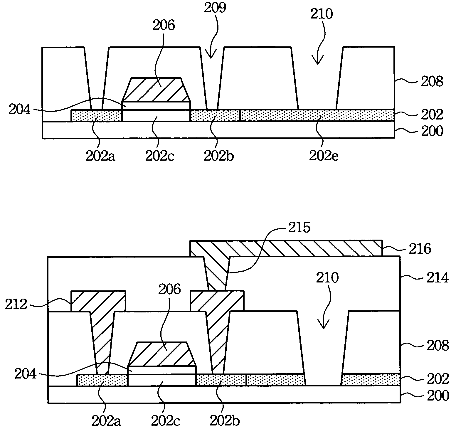
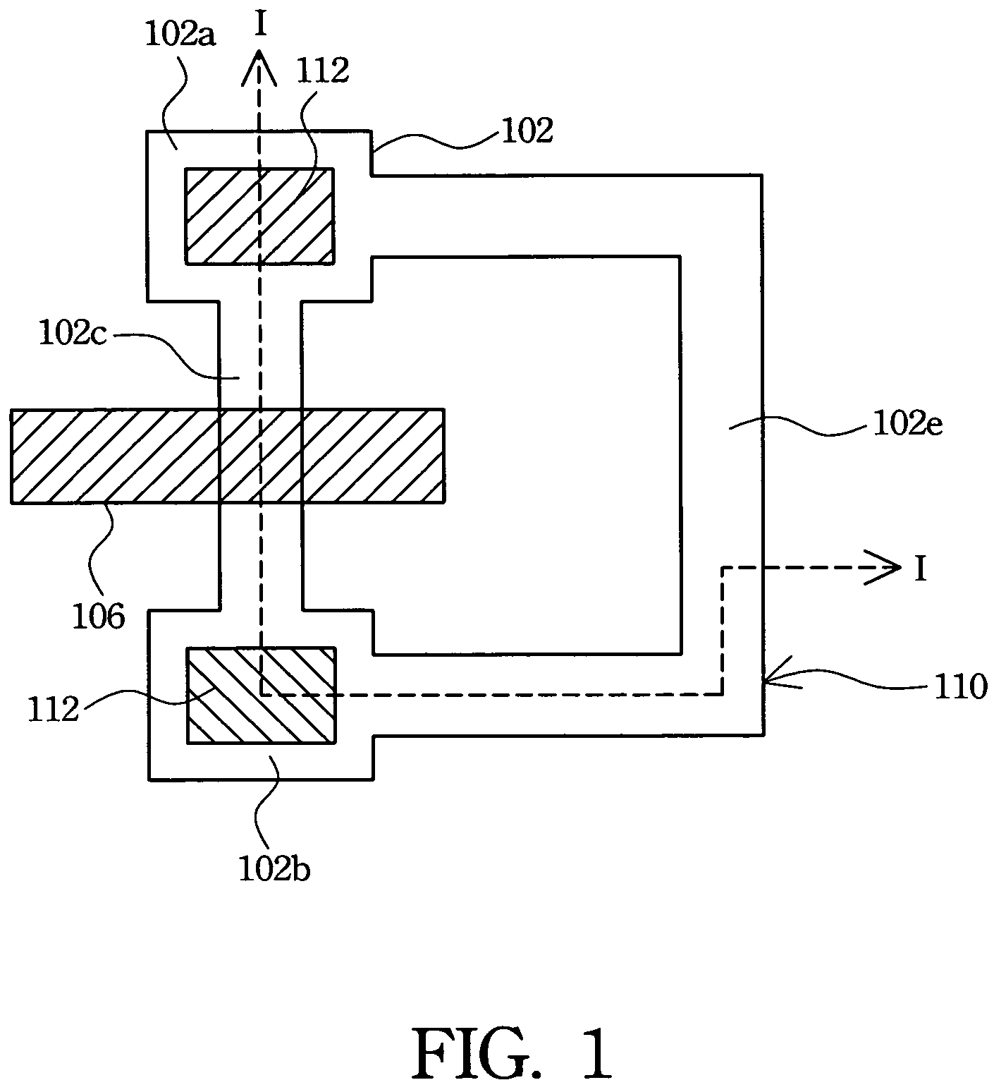
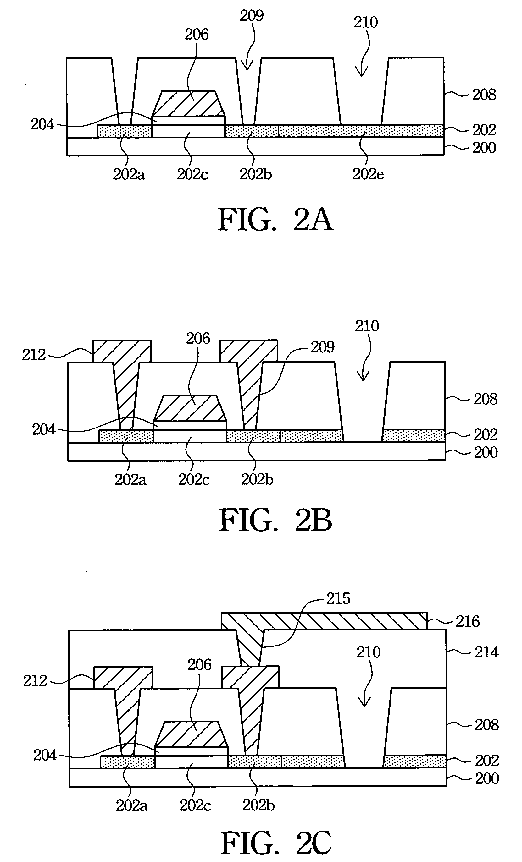
[0022]The present invention discloses a method of forming TFT devices with ESD protection and a structure thereof. Referring to FIG. 1 and FIGS. 2A–2C respectively. FIG. 1 is a top view of a TFT in accordance with the first preferred embodiment of the present invention, and FIGS. 2A–2C are cross-sectional schematic diagrams showing the process for forming the TFT in accordance with the first preferred embodiment of the present invention. The cross-sectional structure shown in FIGS. 2A–2C is taken along line I—I in FIG. 1.

[0023]A source region is connected with a drain region to form a short circuit by utilizing a pattern design for a poly-Si layer. Referring to FIG. 1, in addition to the source region 102a, the drain region 102b and a channel region 102c, a connector 102e connecting the source region 102a and the drain region 102b is also formed in the poly-Si layer 102 to construct the short circuit for dispersing static electricity accumulated in TFT fabrication. Further, a gate e...

embodiment 2

[0033]The present invention discloses another method of forming TFT devices with ESD protection and a structure thereof. Reference is made to FIG. 3, FIG. 4 and FIGS. 5A–5C respectively. FIG. 3 is a partial array structure of the display devices in accordance with the second preferred embodiment of the present invention, FIG. 4 is a top view of TFT devices in accordance with the second preferred embodiment of the present invention, and FIGS. 5A–5C are cross-sectional schematic diagrams showing the process for forming the TFT devices in accordance with the second preferred embodiment of the present invention. The cross-sectional structure shown in FIGS. 5A–5C is taken along line II—II in FIG. 4.

[0034]A TFT in a pixel is connected electrically with another TFT in another pixel by pattern design for a poly-Si layer to form a short circuit. Referring to FIG. 3, regions controlled by data lines 318 and scan lines 319 represent pixels, and a TFT 322 in a pixel 320 is connected with a TFT ...

embodiment 3

[0042]Because ESD protection is achieved by the first embodiment or the second embodiment for forming TFT devices, the present invention discloses further a method of forming TFT devices with ESD protection by combining the first embodiment and the second embodiment for optimized ESD protection.

[0043]Reference is made to FIG. 6 and FIG. 7, respectively. FIG. 6 is a partial array structure of the display devices in accordance with the third preferred embodiment of the present invention, and FIG. 7 is a top view of TFT devices in accordance with the third preferred embodiment of the present invention.

[0044]A source region is connected electrically with a drain region in each TFT to form short circuits, and a TFT in a pixel is also connected electrically with another TFT in another pixel to form another short circuit. Referring to FIG. 6, regions controlled by data lines 618 and scan lines 619 represent pixels, and a TFT 622 in a pixel 620 is connected electrically with a TFT 642 in a ...


PUM

PropertyMeasurementUnit
currentaaaaaaaaaa
voltageaaaaaaaaaa
resolution lossaaaaaaaaaa

Abstract

A silicon layer is formed on a substrate, and then the silicon layer is patterned, and source regions, drain regions and connectors, all with the same conductivity, are formed. The source regions are connected with the drain regions electrically by the connectors, and short circuits are thus constructed. Then, subsequent procedures of thin film transistor fabrication are performed in turn. Finally, when the source / drain metal is patterned to form data lines, the connectors are cut off by etching as the source / drain metal is etched.

Description

FIELD OF THE INVENTION[0001]The present invention relates to a method of forming thin-film transistor devices, and more particularly, to a method of forming thin-film transistor display devices with electro-static discharge protection.BACKGROUND OF THE INVENTION[0002]Thin film transistor (TFT) has been employed for driving an active matrix liquid crystal display (AMLCD) generally, but accumulation of static electricity is usually produced in fabricating thin film transistors because a glass substrate used for display is an insulator, and electro-static accumulation issues easily result in device damage and greatly reduce product yield.[0003]Static electricity is usually generated from the process environment in thin film transistor fabrication, such as in the chemical vapor phase deposition (CVD), sputtering or plasma dry etching process. In addition, static electricity accumulation is also produced from outside conditions in process transition or substrate transmission. Static elec...

Claims


Application Information

Patent Timeline
Patent Type & Authority Patents(United States)
IPC IPC(8): H01L21/00H01L21/84H01L21/77H01L23/60H01L27/01H01L27/02H01L27/12H01L29/10H01L29/78
CPCH01L27/124H01L27/12H01L27/0248
Inventor CHEN, CHEN-MINGCHU, FANG-TSUNCHANG, JIUN-JYE
Owner TRANSPACIFIC IP LTD
Learn More